引脚描述
CI1312芯片引脚图如图P-1所示:
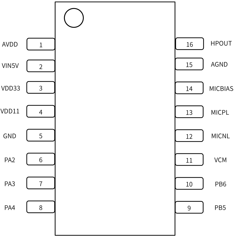
图P-1 芯片引脚图
芯片各个引脚功能如下表描述:
表P-1 芯片引脚功能描述
| Pin Number | Pin name | Pin type | IO 5V-Tolerant | IO power-on default state | Description and alternate functions |
|---|---|---|---|---|---|
| 1 | AVDD | P | - | - | 3.3V output or 3.3V analog power supply, output capacitance/input capacitance is 4.7uF |
| 2 | VIN5V | P | - | - | VIN5V is the PMU power supply input pin. The normal working input voltage range is 3.6V-5.5V. A 4.7uf input capacitor is connected externally. The maximum input voltage of this pin is 6.5V. Note that overvoltage and surge protection devices need to be added, such as a TVS and a 4.7 ohm resistor to protect against surge impact |
| 3 | VDD33 | P | - | - | 3.3V output, output capacitance/input capacitance is 4.7uF |
| 4 | VDD11 | P | - | - | 1.1V output or 1.1V Power supply, output apacitance/input capacitance is 4.7uF |
| 5 | GND | P | - | - | Ground PAD |
| 6 | PA2 | IO | √ | IN,T+D | 1. GPIO PA2(Initial state at startup) 2. IIC_SDA 3. UART1_TX 4. PWM0 |
| 7 | PA3 | IO | √ | IN,T+D | 1. GPIO PA3(Initial state at startup) 2. IIC_SCL 3. UART1_RX1 4. PWM1 |
| 8 | PA4 | IO | √ | IN,T+U | 1. GPIO PA4(Initial state at startup)/PG_EN(Note1) 2. PWM2 |
| 9 | PB5 | IO | √ | IN,T+U | 1. GPIO PB5(Initial state at startup) 2. UART0_TX 3. IIC_SDA 4. PWM1 |
| 10 | PB6 | IO | √ | IN,T+U | 1. GPIO PB6(Initial state at startup) 2. UART0_RX 3. IIC_SCL 4. PWM2 |
| 11 | VCM | O | - | - | VCM Output |
| 12 | MICNL | I | - | - | Left Microphone N input |
| 13 | MICPL | I | - | - | Left Microphone P input |
| 14 | MICBIAS | O | - | - | Microphone bias output |
| 15 | AGND | P | - | - | Analog ground |
| 16 | HPOUT | O | - | - | DAC output |
上表中 IO引脚的状态定义如下:
I 输入
O 输出
IO 双向
P 电源或地
T+D 三态正下拉
T+U 三态正上拉
OUT 上电默认为输出模式
IN 上电默认为输入模式
所有IO支持驱动能力可配,上下拉电阻可配。
Note1:PA4(PG_EN)引脚根据上电时电平状态判断是否进行编程,高电平时启动编程功能。