CI-E0XGT02S Module Datasheet
Module Introduction
Overview
The CI-E0XGT02S is an intelligent voice AIoT module developed by Chipintelli. At its core, this module utilizes Chipintelli’s new generation of high-performance neural network intelligent voice chip series CI230X, which integrates Chipintelli’s self-developed Brain Neural Processing Unit (BNPU V3) and CPU core, along with Wi-Fi and BLE Combo functionality. The system can reach a main frequency of 220MHz, features built-in large-capacity SRAM, integrates PMU power management unit, dual-channel high-performance low-power Audio Codec, and multiple peripheral control interfaces including UART, I2C, IIS, PWM, and GPIO. The chip also integrates PA/LNA/TRX Switch.
The CI-E0XGT02S module supports the standard IEEE 802.11 b/g/n protocol and BLE 5.1 wireless communication protocol, along with protocol stacks such as TCP/UDP, HTTP/HTTPS, PING, and MQTT. It only requires a small number of peripheral components like resistors and capacitors to implement various intelligent voice offline/online product hardware solutions, offering excellent cost performance.
The CI230X series chips are designed to industrial-grade standards, offering high environmental reliability. They operate within a temperature range of -40°C to +85°C, comply with MSL3 moisture sensitivity level, meet the IEC 61000-4-2 standard for 4KV contact discharge testing, and adhere to FCC electromagnetic compatibility standards, as well as ROHS and REACH environmental protection standards.
The CI230X series chips incorporate Chipintelli’s V3 BNPU technology, supporting neural networks such as DNN, TDNN, and RNN, along with convolutional operations. They enable voice recognition, voiceprint recognition, voice enhancement, and voice detection, featuring powerful acoustic echo cancellation and environmental noise suppression capabilities that outperform other voice chips. The chip solution also supports multiple languages including Chinese, English, and Japanese, making it widely applicable in home appliances, lighting, toys, wearables, industrial, automotive, and other product fields for voice interaction, control, and various intelligent voice applications.
The CI230X series currently includes two chip models: CI2305 and CI2306. These two chips are pin-to-pin compatible, differing only in their built-in Flash memory capacity. The CI2305 comes with 4MB of built-in Flash, while the CI2306 features 6MB. Due to its smaller Flash capacity, the CI2305 only supports offline voice recognition and AIoT applications with IoT connectivity. In contrast, the CI2306 supports both offline and online voice recognition, accommodates larger neural network models, offers more voice prompts, and delivers superior noise reduction performance.
The CI-E0XGT02S module is available in two models: CI-E05GT02S and CI-E06GT02S. These models are pin-to-pin compatible, with the only difference being the main chip. The CI-E05GT02S uses the CI2305 chip, while the CI-E06GT02S uses the CI2306 chip. The model selection table is as follows:
| Module model | Main chip | Flash capacity | Applications |
|---|---|---|---|
| CI-E05GT02S | CI2305 | 4MB | AIOT |
| CI-E06GT02S | CI2306 | 6MB | Offline&online speech recognition |
Key Features
-
Single chip IEEE 802.11 b/g/n Wi Fi SOC module, supporting AIOT and offline&online applications.
-
Built in PA/LNA/TRX switch.
-
Support STA/AP/STA+AP mode.
-
Built in protocol stack: TCP/UDP/HTTP/HTTPS/PING/MQTT, TLS support for TCP/UDP.
-
Support Bluetooth LE 5.1, long range (125Kbps, 500Kbps) and high transmission rate (2Mbps).
-
The hardware BNPU is used for neural network operation, and the BNPU is upgraded to V3 version to enhance AI voice processing function, support DNN/TDNN/RNN and other neural networks and convolution operations, and support voice recognition, voiceprint recognition, voice enhancement, voice detection and other functions.
-
Built in 32-bit high-performance CPU, support up to 220MHz operating frequency, 32-bit single cycle multiplier, and support DSP extension.
-
Built in large capacity SRAM, built-in 512bit eFuse, and built-in 4/6MB Flash.
-
Built in high-performance low-power Audio Codec module, supporting dual ADC sampling and single DAC playback; Support the Automatic Level Control (ALC) function; Support 8kHz/16kHz/24kHz/32kHz/44.1kHz/48kHz sampling rate; Support one IIS audio extension channel; It supports PDM interface, and can dock single or two digital MEMS microphones.
-
Multiple high-performance LDOs are built in, and only one power supply device is needed for the periphery to work. It supports direct 5V power input, with a wide input voltage range from 3.6V (minimum) to 5.5V (maximum).
-
Built in AES-128/AES-192/AES-256 hardware encryption and decryption, and built-in true random number generator.
-
One 12bit SAR ADC input channel is supported, and the sampling frequency can reach 1MHz.
-
Supports 2 UART interfaces with baud rates up to 3Mbps; includes 1 I2C interface for connecting external I2C devices; features 6 PWM interfaces for direct drive applications like lighting control and motor control; integrates 4 sets of 32-bit timers; includes 1 independent watchdog timer (IWDG) and 1 window watchdog timer (WWDG).
-
Supports 18 high-speed GPIOs with configurable interrupt functionality; some GPIOs support direct communication with 5V level signals without requiring external level shifting.
-
Provide complete software development package, application solution examples and voice development platform online firmware production and other functions. For details, please visit:( https://aiplatform.Chipintelli.com )
-
Support UART upgrade and firmware protection.
-
Good EMC design, support FCC standard, internal ESD enhanced design, and pass 4KV contact discharge test.
-
Adopt environment-friendly materials and support ROHS and REACH tests.
-
The module is small in size, and the packaging form is SMD-31. The size is 24mm long, 16mm wide, and 3mm high (including the shielding cover).
-
Ambient working temperature: - 40 ℃ to 85 ℃.
Main Parameters
| Module model | CI-E0XGT02S |
|---|---|
| Packaging | SMD-31 |
| Size | 24 * 16 * 3.0mm (dimensional tolerance ± 0.2) |
| Antenna | On board PCB antenna |
| Frequency band range | 2412 ~ 2484 Mhz |
Power supply range |
5V: power supply voltage 3.6~5.5V, power supply current ≥ 500mA 3.3V: power supply voltage 2.6~3.6V, power supply current ≥ 1A |
| Support interfaces | UART、GPIO、ADC、PWM、I2C、I2S、PDM、MIC、HPOUT |
Number of GPIO |
18 GPIOs: PE2, PE3, PE9, PA2, PA3, PA4, PA5, PA6, PA7, PB0, PB1, PB2, PB3, PB4, PB5, PB6, PF4, PF5 |
| Serial port rate | The maximum support is 3000000 bps, and the default is 921600 bps |
| Bluetooth | BLE 5.1 |
| Security encryption | WEP/WPA-PSK/WPA2-PSK |
Flash |
CI-E05GT02S:4MB CI-E06GT02S:6MB |
| Operating temperature | -40℃ ~ 85℃ |
| Storage environment | -40℃ ~ 100℃,≤ 5% RH |
Electrical Parameters
Electrical Characteristics
| Symbol | Parameter | Minimum | Typical | Maximum | Unit |
|---|---|---|---|---|---|
| 5V_IN | PMU input pin voltage generally 5V |
3.6 | 5 | 5.5 | V |
| VDD33 | Wi Fi power supply voltage | 2.6 | 3.3 | 3.6 | V |
| VIH | Input high voltage 3.0V ≤ VDD33 ≤ 3.6V |
VDD33-0.6 | / | VDD33+0.3 | V |
| VIL | Input low voltage 3.0V ≤ VDD33 ≤ 3.6V |
/ | / | 0.6 | V |
| VOL | Output low voltage @ IOL=12mA | / | / | 0.4 | V |
| VOH | Output high voltage @ IOL=20mA | VDD33-0.5 | VDD33 | VDD33+0.3 | V |
| I3.3V | Working current of 3.3V power supply of module | 90 | / | 500 | mA |
| I5V | Working current of 5V power supply of module | 55 | / | 250 | mA |
WiFi Features
Supported frequency band
| Parameter | Min | Typ | Max | Unit |
|---|---|---|---|---|
| Receive frequency rang 2.4Ghz | 2412 | / | 2484 | Mhz |
Receiving characteristics
| Parameter | Condition | Min | Typ | Max | Unit |
|---|---|---|---|---|---|
| Sensitivity | |||||
| 11b,1M | FER < 8%,1024 bytes | / | -94 | / | dBm |
| 11b,11M | FER < 8%,1024 bytes | / | -87 | / | dBm |
| 11g,6M | FER < 10%,1024 bytes | / | -90 | / | dBm |
| 11g,54M | FER < 10%,1024 bytes | / | -74 | / | dBm |
| 11n,MCS0 | FER < 10%,1024 bytes | / | -90 | / | dBm |
| 11n,MCS7 | FER < 10%,1024 bytes | / | -71 | / | dBm |
| Maximum input level | |||||
| 11b | FER < 8%,1024 bytes |
/ | 4 | / | dBm |
| 11g | FER < 10%,1024 bytes |
/ | -10 | / | dBm |
| 11n | FER < 10%,1024 bytes |
/ | -10 | / | dBm |
| power consumption | |||||
| 11b | / |
/ | 80 | / | mA |
| 11g | / |
/ | 82 | / | mA |
| 11n | / |
/ | 82 | / | mA |
Note: The above power consumption data is the current measured when VDD33 is 3.3V.
Emission characteristic
| Parameter | Condition | Min | Typ | Max | Unit |
|---|---|---|---|---|---|
| Output power | |||||
| 11b,1M DSSS | Maximum Burst power | / | 18 | / | dBm |
| 11g,54M OFDM | Maximum Burst power | / | 16 | / | dBm |
| 11n,MCS7 | Maximum Burst power | / | 14 | / | dBm |
| Power consumption | |||||
| 11b | 100% Duty Cycle @ 17dBm |
/ | 320 | / | mA |
| 11g | 100% Duty Cycle @ 14dBm |
/ | 290 | / | mA |
| 11n | 100% Duty Cycle @ 13dBm |
/ | 270 | / | mA |
Note: The above power consumption data is the current measured when VDD33 is 3.3V.
Module Specifications
External Dimensions

As shown in Figure 2, the user can design the structure according to this size, in mm.
Pinout Diagram
The function description of all external pins of the module is shown in Table 7:
Table 7 Comparison Table of Module Pins
| Pin number | Pin name | Type | IO 5V Withstand voltage | Power on default Status recognition | Pin reuse Function description |
|---|---|---|---|---|---|
| 1 | RSTn | I | - | - | Reset pin |
| 2 | PE2 | IO | - | IN,PU | 1.GPIO PE2 2.WIFI firmware download TX |
| 3 | PE3 | IO | - | IN,PU | 1.GPIO PE3 2.WIFI firmware download RX |
| 4 | PE9 | IO | - | IN,PU | 1.GPIO PE9 2.WIFI BOOTMODE1 |
| 5 | AIN2 | IO | - | IN,T+U | 1.GPIO PC4(power on default state) 2.IIC_SCL 3.PWM0 4.PDM_CLK 5.SAR ADC input channel 2 |
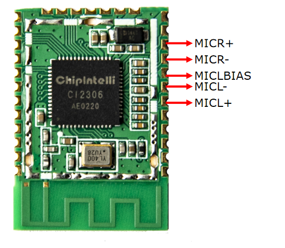
| 6 | MICL+ | I | - | - | Left Microphone P input |
| 7 | MICL- | I | - | - | Left Microphone N input |
| 8 | MICBIAS | O | - | - | Microphone bias output |
| 9 | MICR- | I | - | - | Right Microphone N input |
| 10 | MICR+ | I | - | - | Right Microphone P input |
| 11 | HPOUTL- | O | - | - | DAC output |
| 12 | AGND | P | - | - | Analog ground |
| 13 | 5V_IN | P | - | - | 5V power input, external 4.7uf and 0.1uF capacitors |
| 14 | GND | P | - | - | GND |
| 15 | VDD33 | P | - | - | 3.3V power input, external 4.7uf and 0.1uF capacitors |
| 16 | PA2 | IO | √ | IN,T+D | 1.GPIO PA2 (default state of power on) 2.IIS_SDI 3.IIC_SDA 4.PWM0 |
| 17 | PA3 | IO | √ | IN,T+D | 1.GPIO PA3(Power-on default state) 2.IIS_LRCLK 3.IIC_SCL 4.PWM1 |
| 18 | PA4 | IO | √ | IN,T+U | 1.GPIO PA4 (power on default state)/PG_EN (judge whether to program according to the level state at power on, and start the programming function at high power level)2.IIS_SDO 3.PWM2 |
| 19 | PA5 | IO | √ | IN,T+D | 1.GPIO PA5 (default state of power on) 2.IIS_SCLK 3.PDM_DAT 4.UART2_TX 5.PWM3 |
| 20 | PA6 | IO | √ | IN,T+D | 1.GPIO PA6 (default state of power on) 2.IIS_MCLK 3.PDM_CLK 4.UART2_RX 5.PWM4 |
| 21 | PA7 | IO | √ | IN,T+D | 1.GPIO PA7 (default state of power on) 2.PWM0 3.EXT_INT[0] |
| 22 | PB0 | IO | √ | IN,T+D | 1.GPIO PB0 (default state of power on) 2.PWM1 3.EXT_INT[1] |
| 23 | PB1 | IO | √ | IN,T+D | 1.GPIO PB1 (default state of power on) 2.PWM2 3.UART2_TX |
| 24 | PB2 | IO | √ | IN,T+D | 1.GPIO PB2 (default state of power on) 2.PWM3 3.UART2_RX |
| 25 | PB3 | IO | √ | IN,T+D | 1.GPIO PB3 (default state of power on) 2.PWM4 3.IIC_SDA |
| 26 | PB4 | IO | √ | IN,T+D | 1.GPIO PB4(Power-on default state) 2.PWM5 3.IIC_SCL |
| 27 | PB5 | IO | √ | IN,T+U | 1.GPIO PB4 (default state of power on) 2.UART0_TX 3.IIC_SDA 4.PWM1 |
| 28 | PB6 | IO | √ | IN,T+U | 1.GPIO PB5 (default state of power on) 2.UART0_RX 3.IIC_SCL 4.PWM2 |
| 29 | PF4 | IO | - | IN,PU | GPIO PF4 |
| 30 | PF5 | IO | - | IN,PU | GPIO PF5 |
| 31 | GND | P | - | - | GND |
Note 1: All IOs support configurable drive strength and pull-up/down resistors.
***Note 2: The primary function of all multiplexed pins is their default configuration upon power-up. ***
Note 3: The module will automatically enter upgrade mode if upgrade signals are detected on PB5/PB6 during power-up.
Note 4: The module package includes a thermal pad on the bottom that must be grounded in the application design.
Some symbols in the above table are described as follows:
I input
O output
IO bidirectional
P power or ground
T+D tri-state plus pull-down
T+U tri-state plus pull-up
OUT power-on defaults to output mode
Module Schematic Diagram
Circuit Design Reference
Power Supply
-
The module’s VIN_5V is the 5V power supply input pin with a ripple requirement of <100mV. 5V is the typical operating voltage, and input voltage exceeding 5.5V may potentially damage the module. During audio playback, the maximum 5V current can reach 250mA (including an external 4Ω/3W speaker). As a general principle, a power supply with 500mA driving capability should be provided with double the margin. Additionally, a 4.7Ω 0805 package resistor must be connected in series to the module’s VIN_5V pin to form a surge protection circuit with the internal TVS diode - this must not be omitted.
-
The module’s VDD33 is the 3.3V power supply input pin and requires a separate power supply. It is recommended to use a DCDC converter, such as the RY3408 DCDC chip. Users may also select their own DCDC chip according to their specific requirements. The DCDC chip must have a current driving capability of >1A.
-
For FCC/CE EMI certification testing requirements, it’s recommended to reserve 100pF grounding capacitors for both VIN_5V and VDD33, placed close to the module pins.
-
If the input power ripple is significant, additional measures such as electrolytic capacitors should be added to improve ripple performance.
-
Power and ground traces should be as wide as possible, recommended >15mil.
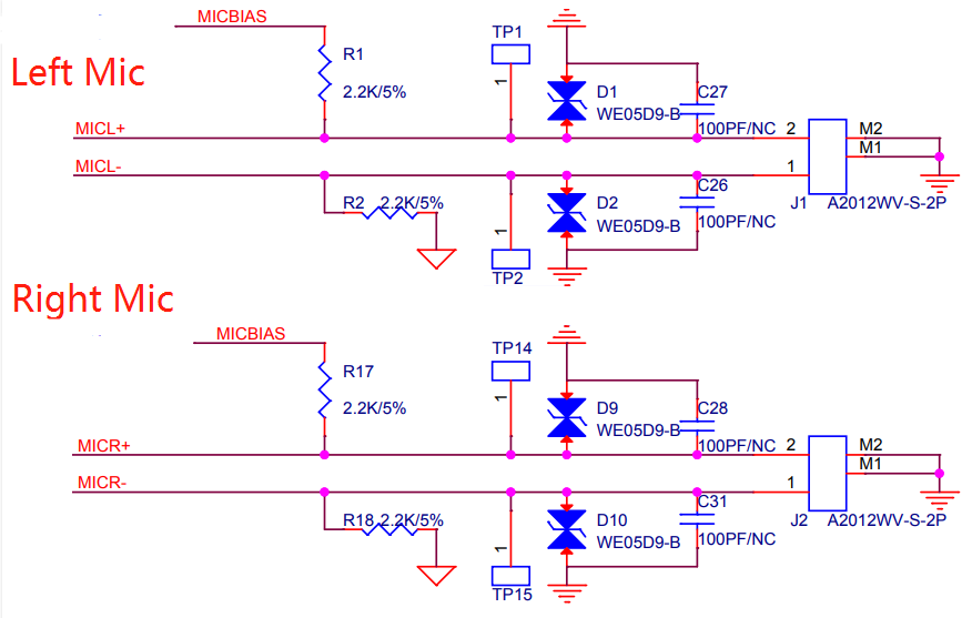
Microphone
- The module supports single or dual microphone input.
- The module has integrated coupling capacitors internally, eliminating the need for external circuits.
- ESD protection devices must be placed at the MIC input port to ensure ESD performance.
- For FCC/CE EMI certification testing requirements, reserve 100pF grounding capacitors on the MIC signal lines.
- Place ESD protection close to the input socket, with the trace routing through the ESD device before reaching the grounding capacitor.
- If there are traces between the ESD device and the signal end, the trace width should be at least 20 mils.
- Use more than 3 ground vias at the connection point between the ESD device and DGND to enhance grounding.
- Keep MIC signal traces as short as possible, routed on the same layer without layer changes.
- Other signal traces should be kept away from MIC traces.
- Enclose MIC traces with AGND on both sides and place AGND copper pour beneath the trace area.
- The MIC input socket must be clearly labeled with left/right channel silkscreen and positive/negative terminal markings according to the circuit connection. Implement measures to prevent reverse polarity connection.
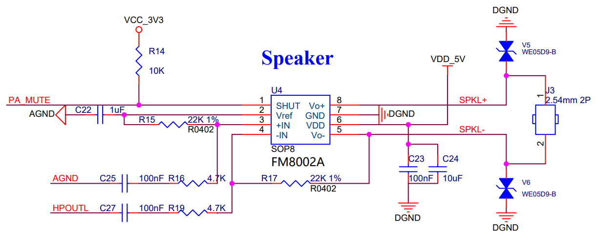
Power amplifier
- Determine the model of power amplifier chip (digital or analog) according to the requirements of the application solution, and design according to the corresponding design reference circuit
- Class AB analog power amplifier is used in this reference design, and the actual application solution determines whether to retain or cancel the ESD device according to the ESD performance requirements of the application solution
- Whether MUTE lines need to place pull-up/pull-down resistors is subject to the definition of power amplifier mute state (if the power amplifier is defined as low-level mute, pull-down resistors need to be placed)
- In this reference design, it is recommended to use PA4 for mute control, with built-in pull-up resistor. If the power amplifier is defined as high-level mute, it is unnecessary to place additional pull-up resistor
- This reference design recommends that AGND and HPOUTL pins be connected to the power amplifier by differential wiring to avoid abnormal noise caused by audio interference
AEC
- The module supports single microphone + AEC application and double microphones + AEC application
- Single microphone + AEC solution: the microphone is connected to the left channel, and the output signal of the power amplifier SPKL+ or SPKL- is transmitted back to MICP_R after being divided by the voltage dividing circuit.

- Dual microphones + AEC solution: The microphone is connected to the left and right channels. The output signals of the power amplifier, SPKL+and SPKL -, need to be divided by the voltage divider circuit, then sent to the external ADC circuit. After ADC conversion, they are returned to the module I2S interface
- ADC chip (ES7243E) shall be placed as close to the module as possible
- Punch 2 * 2 vias on the grounding pad below the ADC chip (ES7243E) to ensure good grounding
- The I2S wiring shall be as short as possible to avoid interference signals. It is recommended that the I2S signal line be completely grounded
- The AGND and DGND networks of the ADC chip (ES7243E) are connected at a single point on the B-side of the chip bottom or near the chip
UART
- The module reserves two high-speed UARTs: UART0 and UART2. UART0 is the default interface for voice firmware downloads, while UART2 serves as the communication port for connecting with other systems.
- If there are requirements for FCC/CE and other EMI certification tests, 100pF grounding capacitance and 100Ω series resistance shall be reserved on the UART line
- If there are ESD/EFT performance test requirements, ESD devices shall be reserved on UART lines. When UART0 is used for communication, TVS junction capacitance must be<25 pF to meet the upgrade requirements; When UART2 is used for communication, when the baud rate is 9600, the TVS junction capacitance is required to be<400pF; When the baud rate is 921600, the TVS junction capacitance is required to be<50pF
- If the UART needs to connect to the 5V level communication system, a 5V pull-up resistor should be placed on the UART line, and the software should be set to open drain mode
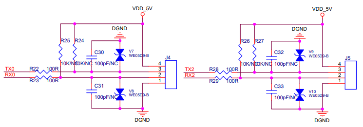
- PE2 and PE3 are COM ports for downloading Wi Fi firmware, and PF4 and PF5 are COM ports for printing Wi Fi Log logs, which are not recommended for other functions
- The function description of the module COM port is shown in Table 8:
| UART | IO 5V withstand voltage | Function description |
|---|---|---|
| UART0 | √ | Voice firmware download, default baud rate 2000000;Voice Log log printing, default baud rate 921600 |
| UART2 | √ | Communication with other systems |
| PE2、PE3 | × | Wi Fi firmware download, the default baud rate is 2000000 |
| PF4、PF5 | × | Wi Fi Log printing, default baud rate 921600 |
Upgrade Enable Circuit
- PA4 is the voice Firmware Update enabled detection pin: enter the upgrade mode at high level; Enter normal startup mode at low level. Built in pull-up resistor, the default is to detect and upgrade after power on

- Test points TP12 and TP13 are placed on PCB BOTTOM layer for automatic upgrade function
- PE9 is the Wi Fi Firmware Update enabling pin detection: enter the upgrade mode at low level; Enter normal startup mode at high level. Built in pull-up resistor, which is powered on and started normally by default
- The module upgrade enabling function is described in Table 9:
| Enable Feet | Configuration | Description | |
|---|---|---|---|
| PA4 |
R6 | R16 | |
| NC | NC | By default, the upgrade signal is first detected during power on detection. The startup time is about 850ms, which is applicable to applications that do not require high startup time |
|
| 2.2K | 2.2K | By default, the system will enter the normal startup mode when it is powered on. The startup time is about 350ms, which is suitable for applications with quick startup requirements If the production line requires firmware flashing, you can short circuit TP12 and TP13 to detect the upgrade signal and flash the firmware after power on |
|
| PE9 |
0 | Wi Fi Firmware Update enable detection pin: enter upgrade mode at low level |
|
| 1 | The Wi Fi Firmware Update enables the detection of pins: enter the normal startup mode at a high level Built in pull-up resistor, it starts normally when powered on by default |
||
Module Dimensions
- It is recommended to design PCB packaging according to the figure below, with the unit of mm. When designing pads, do not increase pads or shrink pads to avoid short circuit which may affect the use of modules

Module Layout Requirements
- During module assembly, the antenna area should be as far away from metal components and strong interference components as possible to avoid affecting the antenna performance
- During module assembly, the antenna area should be as far away from audio devices as possible, such as audio power amplifier, to avoid audio noise
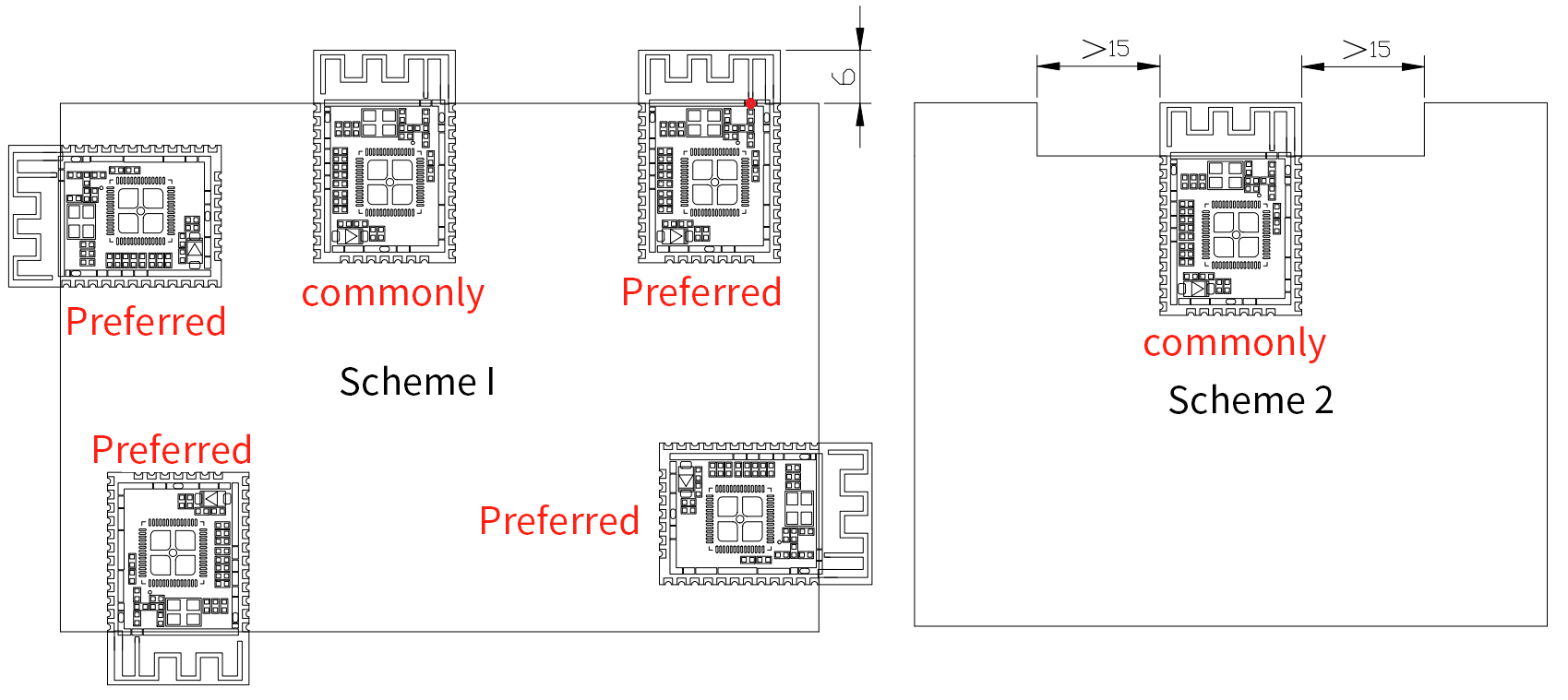
- It is recommended to install the module on the motherboard in the following two ways
- Solution 1: Place the module near the edge of the main board, and the antenna area of the module (including the entire antenna clearance area on the module) must be completely beyond the metal area of the main board PCB. The module antenna area shall extend at least 6mm beyond the mainboard. The preferred position is that the antenna feed point is close to the corner of the main board
- Solution 2: The module antenna area does not extend out of the main board, and the main board in the corresponding area around the antenna is hollowed out. The left and right sides shall be hollowed at least 15mm
Module Application
Power On and Startup
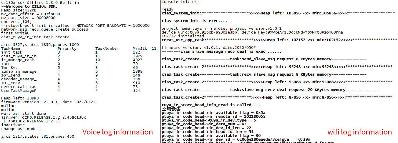
The module has an integrated minimum system. To use it, simply connect the speaker and microphone, then supply 5V and 3.3V power - the module will start automatically. Upon successful power-up, the speaker will play a prompt tone, and print information will appear on the UART0 port. You can connect UART0 to a computer using a USB-to-serial debugging tool. When you see the print information in the serial debugging software, it indicates the module has started successfully.
Note: UART0 serves as both the voice firmware download port and voice log printing port; PE2 and PE3 are for Wi-Fi firmware downloads, while PF4 and PF5 are for Wi-Fi log printing.
Firmware Flashing
Flashing Preparation
Prerequisites
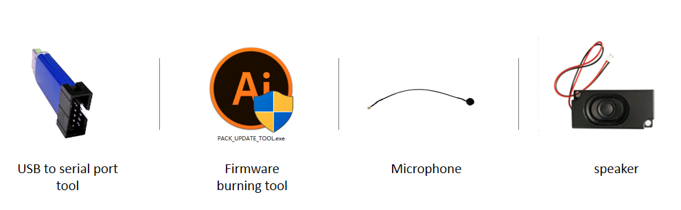
Before programming the module, ensure you have the following components ready:
- Modules to be programmed
- USB-to-UART adapter
- Latest firmware programming tool (pack_update_tool. exe)
- Firmware information (files in *. bin format)
- Microphone with 2.0mm pitch
- 2.5mm pitch speaker
- Several DuPont lines
Hardware Connection and Flashing
Use the USB TYPE-C adapter cable to connect the module and the computer. If there is no backplane as shown in the figure below, the USB-to-UART debugging tool is required, as shown in the USB-to-UART debugging tool above. Before Flashing, connect the power, ground, UART transceiver pins of the USB-to-UART debugging tool with the corresponding pins of the module. Note that the RXD and TXD of the USB-to-UART debugging tool correspond to the UART0_TX and UART0_RX of the module respectively, PE3 and PE2
The wiring diagram of module flashing is shown in the figure below:

Voice Firmware Flashing
- Short circuit the pins at PB5-TX0 and PB6-RX0 with jumper cap
- Switch the onboard UART switch to the “VOICE” position
- Open the firmware programming tool, select the voice firmware programming tag, select the corresponding model according to the chip, click the Firmware Update button, select the prepared firmware file, and find the COM port assigned to the USB-to-UART debugging tool by the corresponding computer. After the preparations are ready, turn on the power switch to automatically enter the programming mode (PA4 internal pull-up), and start downloading firmware. After the download is completed, the progress bar displays 100%
- If the USB-to-UART debugging tool cannot be recognized on the computer, please install the corresponding driver on the computer

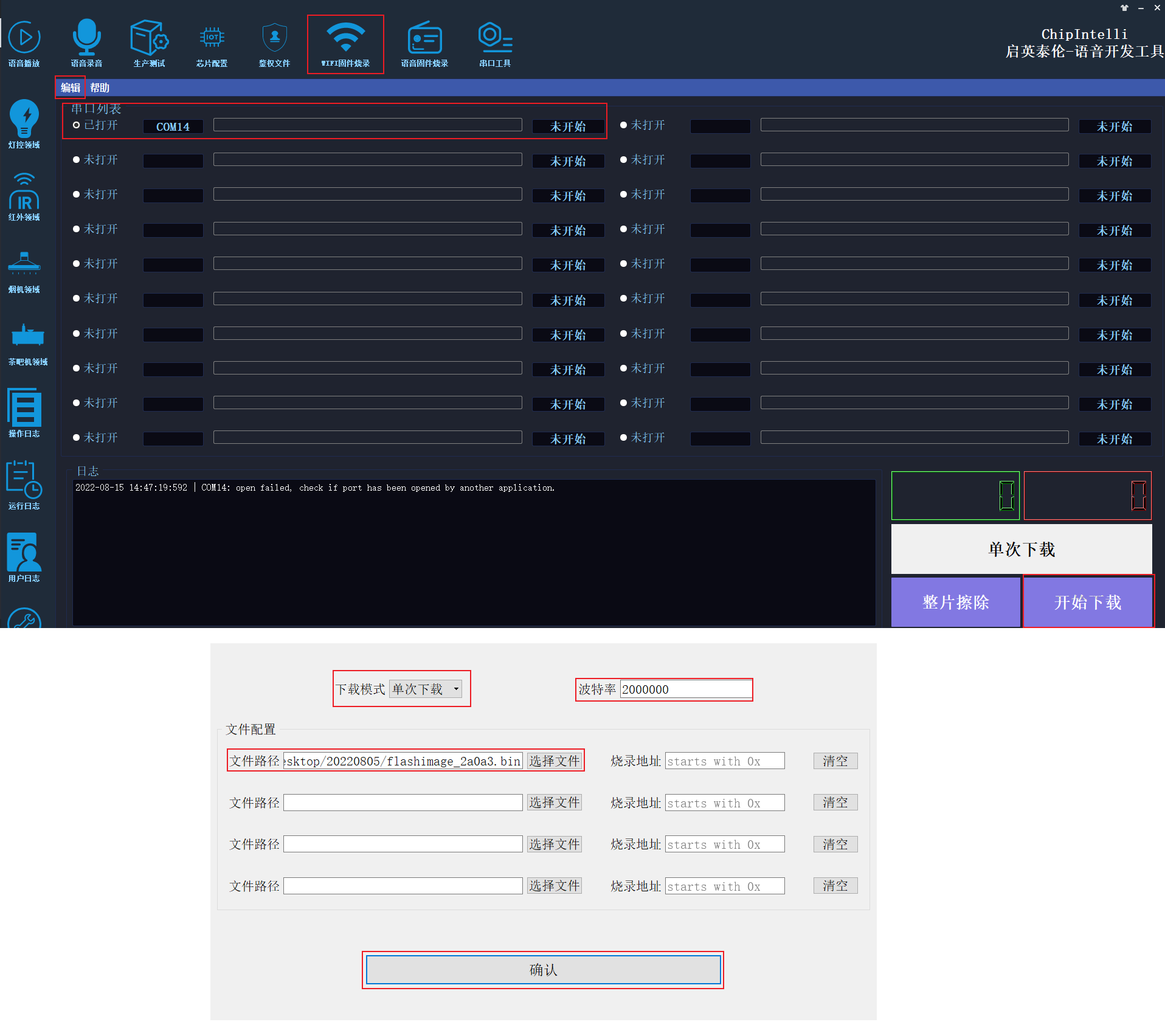
Wi-Fi Firmware Flashing
- Short circuit the pins at PE2, PE3 and PE9 with jumper cap
- Switch the onboard UART switch to the “Wi-Fi” position
- Open the firmware flashing tool, select the WIFI firmware flashing label, set the download mode, firmware file and baud rate in the edit menu, and then confirm. Find the COM port assigned to the USB-to-UART debugging tool by the corresponding computer
- Press and hold the BOOT button. (Pull down PE9)
- Turn on the power switch, click the Start Download button, and enter the Wi Fi firmware download mode. After the download is completed, the progress bar displays 100%
- If the USB-to-UART debugging tool cannot be recognized on the computer, please install the corresponding driver on the computer
Module Test
Function Test after Flashing
After the firmware is successfully flashed, it is recommended to perform a functional test on the module to verify whether the firmware is successfully flashed. During the function test, plug the microphone and speaker into the module to be tested, power on and observe whether it can be normally powered on and broadcast, and use the wake-up word and command word to test whether it can be normally wakened up and recognized. If it can work normally, the module functions normally and the flashing is successful; Otherwise, the flashing fails, and further investigation is required.
Troubleshooting
This chapter lists the problems that may be encountered in the use of some modules and the corresponding solutions
- The module cannot flash and update the firmware. Please check the following operation points:
- Whether PA4 pin has been pulled up and PE9 pin has been pulled down before the module is powered on
- Whether the UART pins are connected correctly, whether the TX and RX are connected reversely, whether the USB-to-UART debugging tool drive at the computer end is normal, and whether the PC flashing tool has selected the correct COM port
- If the above two points are correct, the module cannot be flashed. Use a multimeter to measure whether the power supply voltage of the module is 5V, 3.3V and 1.1V, and use an oscilloscope to measure whether the crystal starts vibrating. Refer to the figure below for each hardware measurement point. If there is a voltage or crystal problem, consider it as a module hardware fault, and replace the module or repair the module hardware. If there is no problem in the above inspection, please contact our technical support personnel for help

- The module is flashed and there is no voice prompt after power on. Please check the following operation points:
- Confirm whether the flashed firmware matches the board
- Make sure the speaker is correctly connected and the power supply is normal
- Check the power amplifier mute pin level, and confirm whether the power amplifier mute pin status matches the power amplifier mute definition
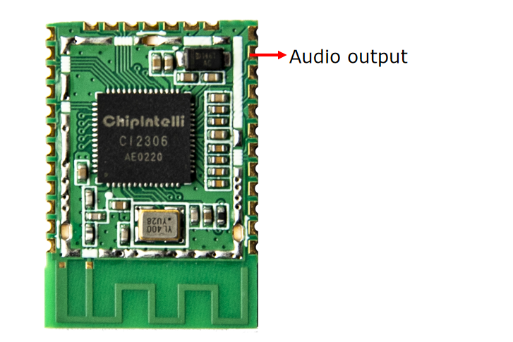
- Use an oscilloscope to measure the voice output test point of the main chip. If there is no output, check whether the firmware is correct. If there is output, check whether the power amplifier components on the module are welded abnormally. If the power amplifier is abnormal, replace it and test again. The measuring points are shown in the figure below. If there is no problem in the above inspection, please contact our technical support personnel for help
- After the module is flashed, there is a voice prompt but the command word is not recognized after power on. Please check the following operation points:
- Check whether the connection between the microphone and the socket is in good condition
- Check whether the positive and negative directions of the microphone are consistent with the markings on the module board and whether they are inserted reversely
- Use a multimeter to measure whether the MICBIAS pin corresponding to the main chip has a voltage of about 2.8V, and use an oscilloscope to measure whether the microphone input pin has an input voice waveform (the voltage of each grid of the oscilloscope is adjusted to the 100mv gear). If the signal is normal, consider whether the firmware is correct, and if the signal is abnormal, observe whether the board hardware has physical damage. The measuring points are shown in the figure below. If there is no problem in the above inspection, please contact our technical support personnel for help
Other Application Precautions
-
The CI230X series chips have a high ESD rating, and the module is designed for easy user expansion, which is why ESD protection devices are only included at the power supply positions on the module. For products with higher ESD requirements, additional ESD protection devices can be added. Please reserve space for ESD protection devices at the corresponding backplane connector positions to ensure product quality and reliability. Users are advised to wear anti-static wrist straps or anti-static gloves and finger cots during inspection and soldering processes.
-
The following networks need to be added with test points and placed on the BOTTOM layer of the main board PCB for mass production automation testing: VCC_5V、VCC3V3、GND、TX0、RX0、TX2、RX2、MIC+、MIC-、SPK+、SPK-、PG_EN.
-
The test points on the main board and module BOTTOM can be hollowed out for RF testing
-
A small resistance, such as 22R, can be connected in series to the communication interface
-
Use the recommended packaging design PCB to avoid poor soldering caused by too much or too little tin
-
When using, pay attention to the microphone, speaker and power supply, and the COM port cannot be connected incorrectly
-
Pay attention to prevent short circuit at the back test point
-
Note that this module must be powered by 5V and 3.3V at the same time, and voice function and Wi Fi function can work normally
-
The user can use the USB to UART debugging tool to debug the developed software. During debugging, add the UART printing command to the corresponding position in the SDK software, generate firmware after compilation and flash it, so as to conduct debugging verification
-
All IOs of this module board are typical 3.3V level, and some IOs also support 5V withstand voltage
-
When designing the module backplane or MCU motherboard, a capacitor with a capacity not less than 100uF shall be placed at the 5V power input of the module; The microphone wiring shall be as short as possible, and the wiring shall be shielded; SPK routing shall be as short and thick as possible, and there shall be no other routing leaps in the routing area
-
Control the warping degree of the bottom plate to be no more than 0.5% to prevent poor module welding
Module Production&Storage Guide, Ordering Information
Production&Storage Guide
-
The packaging module of Chipintelli stamp hole must be mounted by SMT mounting machine, and the mounting must be completed within 24 hours after unpacking, otherwise vacuum packaging shall be carried out again.
-
The storage conditions of Chipintelli stamp hole packaging module are as follows:
- The vacuum moisture-proof bag must be stored in a constant temperature and humidity warehouse with a temperature of 25 ± 5 ℃ and a humidity of 65% ± 10% RH.
- The vacuum moisture-proof bag is equipped with a humidity indicator card, as shown in the figure below:

- Modules delivered from Chipintelli need baking. Humidity indicator card and baking conditions are as follows:
- When unpacking, if 30%, 40% and 50% of the reading value of the humidity indicator card are blue, the module needs to be continuously baked for 2 hours.
- When unpacking, if the humidity indicator card reads that 30% of the color ring turns pink, the module needs to be continuously baked for 4 hours.
- When unpacking, if the humidity indicator card reads that 30% and 40% of the color rings become pink, the module needs to be continuously baked for 6 hours.
- If the humidity indicator card reads that 30%, 40% and 50% of the color rings become pink when unpacking, the module needs to be baked for 12 hours.
- Baking parameters are as follows:
- Baking temperature: 125 ± 5 ℃
- Alarm temperature setting: 130 ℃
- SMT patch can be carried out after cooling under natural conditions<36 ℃
- Drying times: 1 time
- If there is no welding more than 12 hours after baking, please bake again
-
If the unpacking time is more than 3 months, it is prohibited to use the SMT process to weld this batch of modules, because this PCB is a gold deposition process. After more than 3 months, the bonding pad is seriously oxidized, which is very likely to lead to false soldering and missing soldering when SMT is mounted.
-
Before SMT mounting, please conduct ESD (electrostatic discharge, electrostatic discharge) protection on the module. Please wear static gloves and static bracelets during operation.
-
In order to ensure the qualification rate of reflow soldering, all products should be visually inspected and AOI tested to ensure the correctness of furnace temperature control, device adsorption mode and placement mode
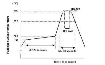
Recommended Reflow Profile
Ordering and Packaging Information
| Product model | Packaging method | Number of modules per pallet | Number of modules per package | Number of modules per box |
|---|---|---|---|---|
| CI-E05GT02S | Tray+electrostatic bag+carton | 140pcs | 15 trays totaling 2100pcs | 3 bags totaling 6300pcs |
| CI-E06GT02S | Tray+electrostatic bag+carton | 140pcs | 15 trays totaling 2100pcs | 3 bags totaling 6300pcs |
Procurement and Technical Support
If the user wants to purchase our product samples, please click on ☞Sample and Bulk Purchase to obtain more information.
If you want to obtain technical support, please log in to ☞Chipintelli AI Speech Development Platform.