Pin Description
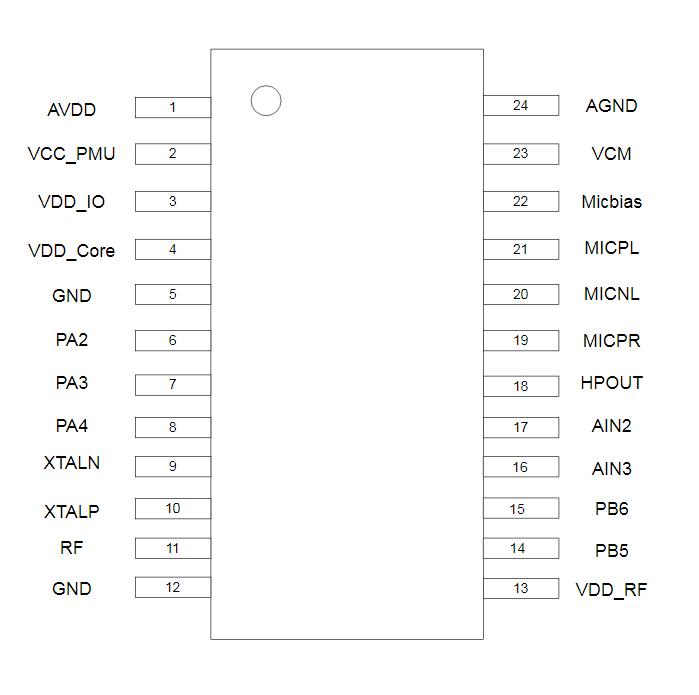
Figure P-1 shows the pin diagram of the CI231 series chip:
Figure P-1 Chip pin diagram
The functions of each pin of the chip are described in the following table:
Table P-1 Describes the functions of chip pins
| Pin Number | Pin name | Pin type | IO 5V-Tolerant | IO power-on default state | Description and alternate functions |
|---|---|---|---|---|---|
| 1 | AVDD | P | - | - | The 3.3V analog LDO output pin is also an analog power supply input pin with an external 4.7uF capacitor |
| 2 | VIN5V | P | - | VIN5V is the PMU power input pin. The normal input voltage ranges from 3.6V to 5.5V. A 4.7uf input capacitor is externally connected. The maximum input voltage of this pin is 6.5V. Please note that this pin requires the addition of overvoltage and surge protection, such as TVS and 4.7 Ω resistor, to prevent surge impact | |
| 3 | VDD33 | P | - | - | 3.3V LDO output pin, external 4.7uF capacitor |
| 4 | VDD11 | P | - | - | The 1.1V LDO output pin is also the core power supply input pin with 4.7uF capacitor |
| 5 | GND | P | - | - | Ground PAD |
| 6 | PA2 | IO | √ | IN,T+D | 1. GPIO PA2(Default power-on status) 2. IIS_SDI 3. IIC_SDA 4. UART1_TX 5. PWM0 |
| 7 | PA3 | IO | √ | IN,T+D | 1. GPIO PA3(Default power-on status) 2. IIS_LRCLK 3. IIC_SCL 4. UART1_RX1 5. PWM1 |
| 8 | PA4 | IO | √ | IN,T+U | 1. GPIO PA4(Default power-on status)/PG_EN(Determine whether to program according to the level state during power-on, and start the programming function at high power times) 2. IIS_SDO 3. PWM2 |
| 9 | XTALN | I | - | - | External crystal oscillator pin positive |
| 10 | XTALP | I | - | - | External crystal oscillator pin negative electrode |
| 11 | RF | - | - | - | RF antenna |
| 12 | GND | P | - | - | Ground PAD |
| 13 | VDD_RF | P | - | VDD_RF is the Bluetooth power input pin. Input voltage is 3.3V. A 4.7uf input capacitor is externally connected. | |
| 14 | PB5 | IO | √ | IN,T+U | 1. GPIO PB5(Default power-on status) 2. UART0_TX 3. IIC_SDA 4. PWM1 |
| 15 | PB6 | IO | √ | IN,T+U | 1. GPIO PB6(Default power-on status) 2. UART0_RX 3. IIC_SCL 4. PWM2 |
| 16 | AIN3 | IO | - | IN,T+U | 1. Reserve(Default power-on status) 2. GPIO PC3 3. PWM1 4.PDM_DAT 5. SAR ADC input channel 3 |
| 17 | AIN2 | IO | - | IN,T+U | 1. Reserve(Default power-on status) 2. GPIO PC4 3. PWM0 4. PDM_CLK 5.SAR ADC input channel 2 |
| 18 | HPOUT | O | - | - | DAC output |
| 19 | MICPR | I | - | - | Right Microphone P input |
| 20 | MICNL | I | - | - | Left Microphone N input |
| 21 | MICPL | I | - | - | Left Microphone P input |
| 22 | MICBIAS | O | - | - | Microphone bias output |
| 23 | VCM | O | - | - | VCM Output |
| 24 | AGND | P | - | - | Analog ground |
The status of the IO pins in the table above is defined as follows:
I input
O output
IO bidirectional
P Power supply or ground
T+D tri-state positive pull-down
T+U tri-state positive pull-up
OUT The default mode is output
IN The default power-on mode is input
All I/O drive capabilities can be configured, and pull-down resistors can be configured.
Note1: PA4 (PG_EN) pin judges whether to program according to the level state at power on, and starts the programming function at high power level
