Hardware Design
The CI1316XP chip requires only a few external components to develop end-product solutions supporting various voice applications. The chip supports single-ended microphone input and mono power amplifier output. The application design can select appropriate circuit solutions based on functional requirements, power consumption, cost, and other factors.
Using the typical application solution of CI13162P as an example, the following outlines the key points and considerations for the application design:
Reference Circuit Diagram
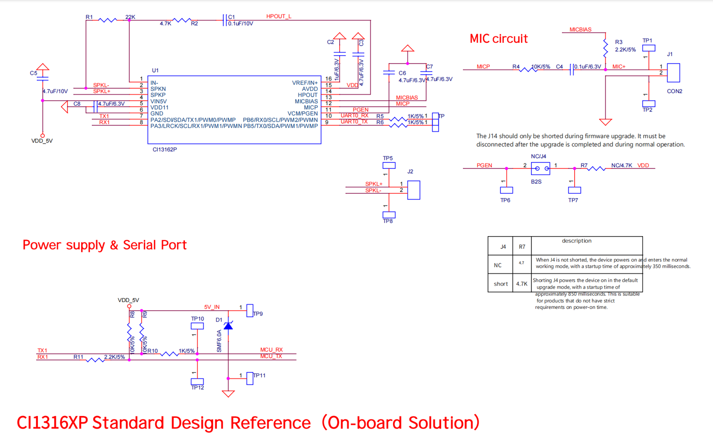
The above diagram shows the reference design circuit for a typical application of the CI1316XP series chips, including CI13162P, featuring single-ended microphone input and power amplifier output. This design is not limited to any specific product. The application design should be based on the principle of adapting to the host terminal product. According to the functional and performance requirements of the end product, please visit the Chipintelli Documentation Center and AI Platform to download reference schematics and PCB layouts. Documentation Center link: https://document.Chipintelli.com/.
If board-level upgrade functionality is required in the application design, the UART0 pins can be brought out via connectors or test points to facilitate firmware programming or upgrades through UART0 after PCB assembly.
The VCM/PGEN pin of C23162 has a built-in pull-down resistor. During power-up, the system detects whether this pin is pulled high to 3.3V by an external pull-up resistor. If it is high and external upgrade signals are detected on the UART0 pins, the system enters upgrade mode. If no external pull-up resistor is connected, the chip can skip the upgrade mode detection and directly enter normal boot mode for faster startup. For applications requiring fast startup, the VCM/PGEN pin can be brought out with a jumper and connected to a 4.7KΩ pull-up resistor to 3.3V. In this configuration, the system boots in normal mode with a startup time of approximately 350ms. For in-system upgrades, the PGEN pin can be pulled high to 3.3V by shorting the jumper or test points, enabling upgrades via the UART0 interface. If fast startup is not required, PGEN can be directly pulled high with a 4.7KΩ resistor. For specific implementation details, please refer to the reference schematic or consult our FAE. The two operating modes of PGEN are as follows:
| J4 Connection | PG_EN Level | Boot Time |
|---|---|---|
| Open | Low Level | 350ms |
| Shorted | High Level | 850ms |
CI13162P supports single-ended microphone input, and the single-ended microphone design shown in Figure H-1 is recommended.
The typical application uses a Class AB power amplifier, with the 8002 series recommended. If voice playback is not required, this circuit can be omitted to reduce costs.
For applications without ultra-low power requirements, it is recommended to use the internal PMU of CI13162P to reduce costs. For ultra-low power applications, an external DCDC circuit can be used to supply 1.1V to CI13162P to reduce system power consumption.
The UART interfaces of CI13162P support 5V level communication. In the figure above, UART0 is shown with 3.3V level communication as an example. For 5V level communication, simply add 5V pull-up resistors to the RX and TX pins of UART0; no level-shifting circuit is required.
PCB Layout Design
Power Circuit
Power Traces
For power input, include overvoltage and surge protection by adding a TVS device and a 1Ω resistor in series with the 5V input. Route the power trace through the TVS first, then through the resistor to the chip. The width of power traces should be determined by the actual current requirements. For 3.3V power, the trace width should be no less than 15 mils; for 1.1V power, the trace width should also be no less than 15 mils. Use copper pours where possible, keep power traces short and wide, and ensure the narrowest section is no less than 8 mils wide. Avoid forming closed loops in power traces.
Power Decoupling Capacitors
Place power decoupling capacitors as close as possible to their corresponding pins.
ESD Protection Requirements
For two-layer board designs, route traces primarily on the TOP layer to maintain the integrity of the BOTTOM ground plane. If ESD protection devices are used, place them as close as possible to the connector pins for optimal protection.
Additional Application Notes
-
CI1316XP is manufactured using lead-free, environmentally friendly materials. When performing SMT soldering, please set the reflow temperature and time parameters according to lead-free standards. A typical SMT soldering temperature profile is shown below:
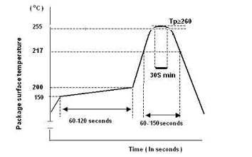 Figure H-2 Chip SMT Soldering Temperature Profile
 -
Take appropriate anti-static measures when handling, transporting, and processing CI1316XP. Use anti-static packaging materials.
-
The chip has a Moisture Sensitivity Level (MSL) of 3. Store the chip under MSL3 conditions before use. If the package has been opened for longer than the MSL3 specification allows, bake the chips before SMT soldering.