Pin Description
The CI1312 chip pin diagram is shown in Figure P-1:
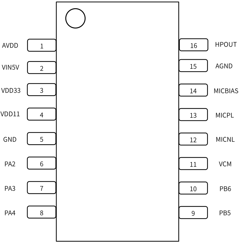
Figure P-1 Chip Pin Diagram
The functions of each pin of the chip are described in the following table:
Table P-1 Chip Pin Function Description
| Pin Number | Pin name | Pin type | IO 5V-Tolerant | IO power-on default state | Description and alternate functions |
|---|---|---|---|---|---|
| 1 | AVDD | P | - | - | 3.3V output or 3.3V analog power supply, output capacitance/input capacitance is 4.7uF |
| 2 | VIN5V | P | - | - | VIN5V is the PMU power supply input pin. The normal working input voltage range is 3.6V-5.5V. A 4.7uf input capacitor is connected externally. The maximum input voltage of this pin is 6.5V. Note that overvoltage and surge protection devices need to be added, such as a TVS and a 4.7 Ω resistor to protect against surge impact |
| 3 | VDD33 | P | - | - | 3.3V output, output capacitance/input capacitance is 4.7uF |
| 4 | VDD11 | P | - | - | 1.1V output or 1.1V Power supply, output apacitance/input capacitance is 4.7uF |
| 5 | GND | P | - | - | Ground PAD |
| 6 | PA2 | IO | √ | IN,T+D | 1. GPIO PA2(Initial state at startup) 2. IIC_SDA 3. UART1_TX 4. PWM0 |
| 7 | PA3 | IO | √ | IN,T+D | 1. GPIO PA3(Initial state at startup) 2. IIC_SCL 3. UART1_RX1 4. PWM1 |
| 8 | PA4 | IO | √ | IN,T+U | 1. GPIO PA4(Initial state at startup)/PG_EN(Note1) 2. PWM2 |
| 9 | PB5 | IO | √ | IN,T+U | 1. GPIO PB5(Initial state at startup) 2. UART0_TX 3. IIC_SDA 4. PWM1 |
| 10 | PB6 | IO | √ | IN,T+U | 1. GPIO PB6(Initial state at startup) 2. UART0_RX 3. IIC_SCL 4. PWM2 |
| 11 | VCM | O | - | - | VCM Output |
| 12 | MICNL | I | - | - | Left Microphone N input |
| 13 | MICPL | I | - | - | Left Microphone P input |
| 14 | MICBIAS | O | - | - | Microphone bias output |
| 15 | AGND | P | - | - | Analog ground |
| 16 | HPOUT | O | - | - | DAC output |
The status of IO pin in the above table is defined as follows:
I Input
O Output
IO bidirectional
P power or ground
T+D tri-state positive pull-down
T+U tri-state positive pull-up
OUT power on defaults to output mode
IN power on default input mode
All IO support drive capacity can be configured, and the up and down resistance can be configured.
Note 1: PA4 (PG_EN) pin judges whether to program according to the level state at power on, and starts the programming function at high power level