GPIO
Function Introduction
The GPIO (General-Purpose Input/Output) interface provides four banks of up to eight programmable pins each (GPIO0⇒PA, GPIO1⇒PB, GPIO2⇒PC, GPIO3⇒PD). Each pin can be independently configured for input or output and has dedicated control and configuration registers.
Features
- Configurable GPIO interrupts with mask control
- Edge-triggered (rising, falling, or both) and level-triggered (high or low) modes
- Individual pin direction control (input/output)
- Separate enable/disable for each pin
IO Multiplexing
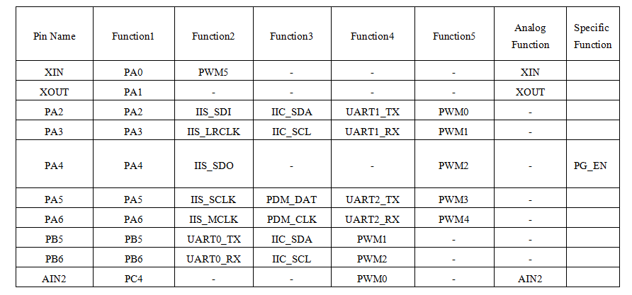
GPIO functions as an alternate function (function 3) via the IO_REUSE_CFG registers in the DPMU module. The reuse relationship is configured by the register IO_REUSE_CFG, please refer to the corresponding contents in the DPMU module for specific description of this register. Please click here to view. The reuse relation is determined by the register IO of the system control unit_REUSE_CFG configuration.. Each set of pin functions needs to be configured with corresponding IO_REUSE_CFG register bit. The analog pin needs to be used as an analog pin or a digital pin according to the reuse situation. The specific reuse relationship is shown in the following figure:
Register Mapping
The base address of GPIO0/½/3 register mapping is 0x40020000, 0x40021000, 0x40031000, 0x40028000. See Table GPIO-1 for each group of registers.
| Offset | Name | Bit Width | Type | Reset Value | Description |
|---|---|---|---|---|---|
| 0x000~0x3FC | GPIODATA | 8 | R/W | 0x00 | Data register |
| 0x400 | GPIODIR | 8 | R/W | 0x00 | Data direction register |
| 0x404 | GPIOIS | 8 | R/W | 0x00 | Interrupt source (level/edge) register |
| 0x408 | GPIOIBE | 8 | R/W | 0x00 | Interrupt source double edge trigger register |
| 0x40C | GPIOIEV | 8 | R/W | 0x00 | Interrupt event register |
| 0x410 | GPIOIE | 8 | R/W | 0x00 | Interrupt mask register |
| 0x414 | GPIORIS | 8 | R | 0x00 | Interrupt original status register |
| 0x418 | GPIOMIS | 8 | R | 0x00 | Interrupt mask status register |
| 0x41C | GPIOIC | 8 | W | 0x00 | Interrupt clear register |
Data Register (GPIODATA)
Offset: 0x000~0x3FC
Reset value: 0x00
| Bit Field | Name | Reset Value | Type | Description |
|---|---|---|---|---|
| 7: 0 | GPIODATA | 0x00 | R/W | GPIO data register When GPIO is configured as input, read this register When GPIO is configured as output, write this register |
Note that this register is used in conjunction with the address offset. One register can be used to perform validity discrimination and specific data operations on 8-bit data of GPIO. Operation mode: The address offset of this register is the address bit [11:0], where [9:2] is a significant bit. If a bit in the address [9:2] is high (set the bit to be bit X), then the corresponding bit (bit X-2) of the corresponding register data [7:0] is valid. If a bit in the address [9:2] is low, then the corresponding bit of the corresponding register data [7:0] is invalid, and reading and writing operations will not affect this bit
For example, if you want to write a 0xFF byte of data to a GPIO port, when the GPIO port has been configured for output, the address offset of this register should be set to 0x3FC, that is, all bits in the address [9:2] should be set to high, and all data bits [7:0] of the GPIO are valid; If only 1 needs to be written to bit 0 of GPIO, the address offset should be set to 0x004. At this time, no matter whether 0x01 or 0xFF is written to this register, only 1 will be written to bit 0 of GPIO, and other bits will not change. The operation is the same when reading.
Data Direction Register (GPIODIR)
Offset: 0x400
Reset value: 0x00
| Bit Field | Name | Reset Value | Type | Description |
|---|---|---|---|---|
| 7: 0 | GPIODIR | 0x00 | R/W | GPIO data direction register 0: input 1: output |
Interrupt Source Register (GPIOIS)
Offset: 0x404
Reset value: 0x00
| Bit Field | Name | Reset Value | Type | Description |
|---|---|---|---|---|
| 7: 0 | GPIOIS | 0x00 | R/W | GPIO interrupt source register 0: edge 1: level |
Interrupt Source Double Edge Trigger Register (GPIOIBE)
Offset: 0x408
Reset value: 0x00
| Bit Field | Name | Reset Value | Type | Description |
|---|---|---|---|---|
| 7:0 | GPIOIBE | 0x00 | R/W | GPIO interrupt source double edge register 0: Interrupt trigger event is controlled by GPIOIEV 1: double edge trigger (GPIOIS is configured as 0) |
Interrupt Event Register (GPIOIEV)
Offset: 0x40C
Reset value: 0x00
| Bit Field | Name | Reset Value | Type | Description |
|---|---|---|---|---|
| 7: 0 | GPIOIEV | 0x00 | R/W | GPIO interrupt event register 0: falling edge or low level 1: rising edge or high level |
Interrupt Mask Register (GPIOIE)
Offset: 0x410
Reset value: 0x00
| Bit Field | Name | Reset Value | Type | Description |
|---|---|---|---|---|
| 7: 0 | GPIOIE | 0x00 | R/W | GPIO interrupt mask register 0: masked interrupt 1: unshielded interrupt |
Interrupt Raw Status Register (GPIORIS)
Offset: 0x414
Reset value: 0x00
| Bit Field | Name | Reset Value | Type | Description |
|---|---|---|---|---|
| 7: 0 | GPIORIS | 0x00 | R | GPIO interrupt original status register. Reflects the interrupt state before masking. |
Interrupt Mask Status Register (GPIOMIS)
Offset: 0x418
Reset value: 0x00
| Bit Field | Name | Reset Value | Type | Description |
|---|---|---|---|---|
| 7: 0 | GPIOMIS | 0x00 | R | GPIO interrupt mask status register. Reflects the interrupt state after the mask. |
Interrupt Clear Register (GPIOIC)
Offset: 0x41C
Reset value: 0x00
| Bit Field | Name | Reset Value | Type | Description |
|---|---|---|---|---|
| 7: 0 | GPIOIC | 0x00 | W | GPIO interrupt clear register 1: Clear the corresponding interrupt status 0: No effect |
Enable Register (GPIOEN)
Offset: 0x420
Reset value: 0x00
| Bit Field | Name | Reset Value | Type | Description |
|---|---|---|---|---|
| 7: 0 | GPIOEN | 0x00 | R/W | GPIO enable register 0: Disable 1: Enable |