Hardware Design
The CI230X chip requires only a few external components to support various online and offline voice applications. For the audio section, the chip supports both dual microphone input and single microphone input with AEC (Acoustic Echo Cancellation) functionality. Users can select the appropriate circuit based on their specific application requirements for functionality, power consumption, and cost. Below is a detailed description of the application reference circuit for single microphone input with AEC echo cancellation.
Application Reference Diagram
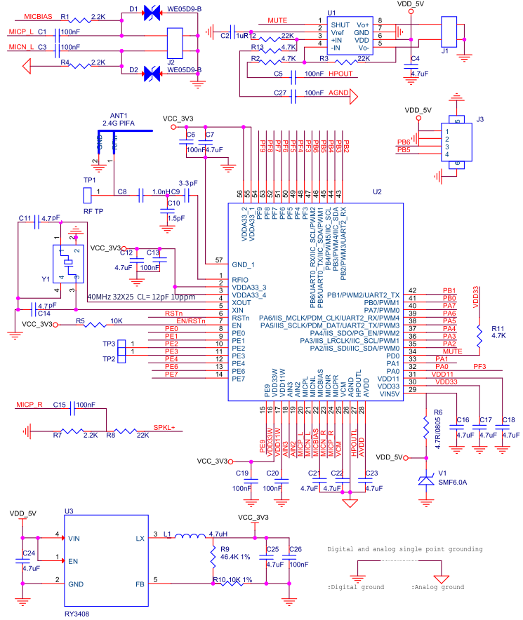
The diagram above shows the application circuit for CI230X supporting single microphone input with AEC echo cancellation and power amplifier output. The chip can be powered directly with 5V, and users can design according to the specifications of the external components shown in the diagram.
If the board-level online upgrade function is to be onsidered during schematic design, the UART0 pin can be led out to facilitate Firmware Update of the flash in the main chip through UART0 after PCB board placement is completed. The PA4 (PG_EN) pin of the chip is internally pulled up, with power-on defaulting to upgrade mode. After power-on, the chip will detect upgrade signals from the external UART0 port and initiate the upgrade process if detected. The default boot time is extended to approximately 850ms due to the upgrade mode detection. If faster boot time is required, the PA4 pin can be configured with two 2.2KΩ pull-down resistors to ground, with a test point between them. In this configuration, the chip will boot in normal mode with a reduced boot time of approximately 350ms. To perform an online upgrade in this configuration, apply a high level to the test point between the 2.2KΩ resistors to pull up the PA4 pin, then proceed with the upgrade via UART0.
Application with this chip can select differential microphone design or single-ended microphone design, and the differential microphone design in the above figure is recommended. If the user has requirements for cost, the microphone part in the above figure can be modified to a single-ended microphone design, which can use fewer passive devices than the differential microphone. However, this method is only recommended for applications where the microphone line length is less than 20 cm, otherwise the speech recognition effect will not be as good as the differential microphone design because the line length is too long and the anti-interference effect is not enough. The power amplifier shown in the figure above is a Class AB amplifier, with the 8002 power amplifier chip recommended in the diagram. Users may select alternative power amplifier chips based on their specific solution requirements. If the power amplifier function is not required, this circuit section can be omitted to reduce costs. For applications requiring AEC, users can utilize a microphone input channel to connect the AEC analog signal input.
If there are no specific power consumption requirements, it is recommended to use the internal PMU for power supply. For applications with strict power consumption requirements, an external DCDC converter can be added to supply 1.1V to the chip to reduce power consumption. All UART ports on the chip support 5V communication. The UART0 port shown in the figure operates at 3.3V. When connecting to 5V interfaces, simply add pull-up resistors to 5V on the RX and TX pins of UART0, with no additional voltage level conversion circuit required.
The VDDA33 and VDD33W pins are the Wi-Fi power supply inputs. The figure shows a DCDC power supply configuration using the recommended RY3408 DCDC chip, though users may select alternative DCDC chips based on their specific requirements. The selected DCDC chip must have a current drive capacity greater than 1A to ensure stable Wi-Fi performance.
Both the RSTn and EN pins can be used to reset the Wi-Fi function, with the EN pin being the recommended choice as shown in the figure. By default, PE2 and PE3 serve as the Wi-Fi firmware download serial ports, while PE9 functions as the download enable pin. To download Wi-Fi firmware, connect PE2 and PE3 to the serial port, pull PE9 low, then power on the chip to enter download mode. The firmware can then be downloaded using the provided software tools.
The crystal oscillator specification for the chip is 40MHz with a load capacitance of 12pF and 10ppm frequency stability. External 4.7pF capacitors must be connected to the XIN and XOUT pins. These specifications are critical and must not be altered. Always adhere strictly to the values shown in the schematic diagram.
The RFIO pin connects to the antenna, with a primary T-type matching network shown in the figure. Users should include both chip-side and antenna-side matching networks based on their specific PCB stack-up and antenna specifications. Note that different PCB layer configurations, antenna types, and assembly environments will require individual tuning of the matching networks to ensure optimal RF performance.
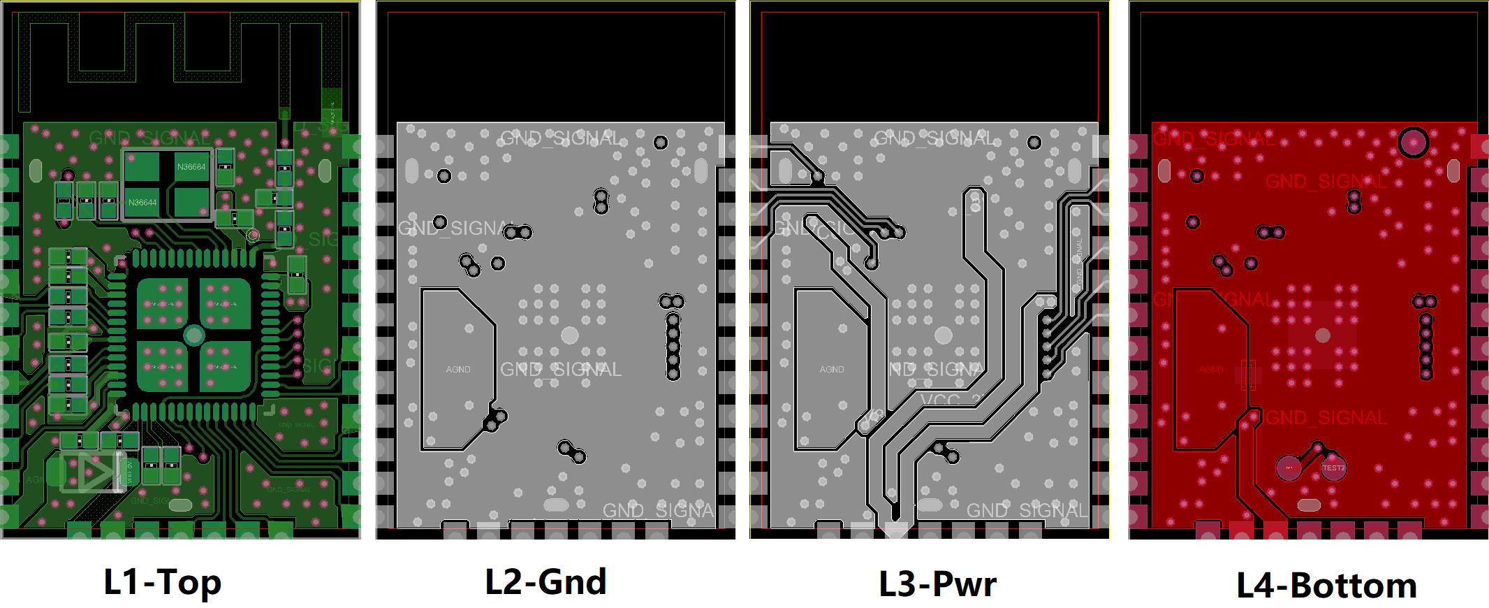
PCB Layout Design
A 4-layer board design is strongly recommended with the following layer stack-up: - Layer 1: Component placement - Layer 2: Continuous ground plane - Layer 3: Power routing and signal traces - Layer 4: Continuous ground plane
This configuration is illustrated in Figure H-2:
Power Circuit
-
The VIN_5V pin is the 5V power supply input with a maximum ripple requirement of 100mV. The typical operating voltage is 5V, and exceeding 5.5V may cause circuit damage. In broadcast mode with an external 4Ω/3W speaker, the maximum current draw can reach 250mA. For reliable operation, the power supply should be capable of providing 500mA (2x margin). A 4.7Ω 0805 resistor must be connected in series with the VIN_5V pin, forming a surge protection circuit in conjunction with the TVS diode. This protection circuit is mandatory and must not be omitted.
-
The VDDA33 and VDD33W pins provide 3.3V power to the Wi-Fi section and require a dedicated power supply. A DCDC converter such as the RY3408 is recommended, though alternative DCDC chips may be used if they meet the minimum 1A current rating. For optimal performance, implement a star routing topology from the power source to pins 2, 3, 55, and 56 (VDDA33) and pin 16 (VDD33W). Maintain ground isolation between these power traces to minimize interference.
-
For FCC/CE and other EMI compliance testing, it is recommended to place 100pF decoupling capacitors close to the VIN_5V and VDD33 pins of the chip.
-
If the input power supply exhibits excessive ripple, additional filtering components such as electrolytic capacitors should be added to reduce ripple to acceptable levels.
-
Power and ground traces should be as wide as possible, with a minimum recommended width of 15 mils.
RF Circuit
-
The RF matching network components must be placed as close as possible to the RFIO pin to minimize trace length and parasitic effects.
-
All RF traces must maintain 50Ω characteristic impedance. Ensure proper ground plane continuity around RF traces, particularly on the top layer.
-
Maintain a clear area around the antenna, keeping it free from ground planes and other components that could affect radiation performance.
Crystal Circuit
-
Ensure the crystal oscillator has a solid ground connection to minimize noise and improve stability.
-
Remove copper pour around the crystal pads on the top layer, and connect the crystal’s ground pin directly to the ground plane (Layer 2) using vias placed as close as possible to the ground pin.
Electrostatic Protection Requirements
Route signals on the top and third layers to preserve the integrity of the ground planes on the second and bottom layers. When ESD protection devices are used, place them as close as possible to the connector pins to maximize their effectiveness.
Other Considerations for Application
- For the CI230X chip, it is recommended to use an external crystal oscillator connected to PA0 and PA1 (12.288MHz crystal circuit). The internal RC oscillator may be considered for cost-sensitive applications where frequency accuracy and temperature range are not critical. However, note that the RC oscillator exhibits temperature drift in extreme temperatures due to semiconductor characteristics. When using the internal RC oscillator, the system clock must be limited to below 220MHz. For applications requiring operation from -40°C to 85°C, an external crystal oscillator is mandatory.
- For applications operating between -10°C to 70°C with low-speed serial communication (baud rate ≤ 115200bps), the internal RC oscillator may be used (with a frequency tolerance of ±1.5%). To minimize communication errors when using the internal oscillator, Chipintelli offers a baud rate adaptation solution. This requires implementing a handshake protocol where the host device must respond within 50ms of receiving the handshake command. With this adaptation, the operational temperature range can be extended to -20°C to 85°C.
- The chip includes a Power Management Unit (PMU) with multiple LDOs that generate 3.3V and 1.1V supplies. The external 5V power supply must maintain ripple below 300mV. For applications with stringent RF performance or power consumption requirements, consider using separate external power supplies for the VDDA33 and VDD33W rails.
- RF performance is highly sensitive to crystal frequency stability. For applications in harsh environments, select a crystal with a wide temperature range specification.
- The RFIO pin requires proper impedance matching. Include a matching network and ensure controlled impedance routing. For longer traces, consider adding a secondary matching network near the antenna.
- For audio output applications, route the AGND and HPOUTL signals differentially to the power amplifier to minimize noise and interference in the audio signal path.
- The chip is manufactured using lead-free processes. During SMT assembly, adhere to lead-free reflow profile specifications for temperature and time parameters.
- Handle all components using proper ESD precautions. Use anti-static packaging and grounding when storing and transporting chips to prevent electrostatic discharge damage.