Pin Description
The CI230X chip pin diagram is shown in Figure P-1:
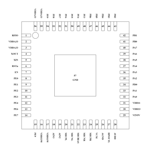
The functions of each pin of the chip are described in the following table:
| Pin Number | Pin name | Pin type | IO 5V-Tolerant | IO power-on default state | Description and alternate functions |
|---|---|---|---|---|---|
| 1 | RFIO | IO | - | - | WIFI RF transmitter/receiver |
| 2 | VDDA33 | P | - | - | 3.3V power input, external 4.7uf and 0.1uf capacitors |
| 3 | VDDA33 | P | - | - | 3.3V power input, external 4.7uf and 0.1uf capacitors |
| 4 | XOUT | O | - | - | 40MHz external crystal pin XOUT |
| 5 | XIN | I | - | - | 40MHz external crystal pin XIN |
| 6 | RSTn | I | - | - | Reset pin |
| 7 | EN | I | - | - | Enable pin |
| 8 | PE0 | IO | - | IN,PU | GPIO PE0 Note1 |
| 9 | PE1 | IO | - | IN,PU | GPIO PE1 Note1 |
| 10 | PE2 | IO | - | IN,PU | 1. GPIO PE2 2.WIFI firmware download TX Note1 |
| 11 | PE3 | IO | - | IN,PU | 1. GPIO PE3 2.WIFI firmware download RX Note1 |
| 12 | PE4 | IO | - | IN,PD | GPIO PE4 Note1 |
| 13 | PE6 | IO | - | IN,PD | GPIO PE6 |
| 14 | PE7 | IO | - | IN,PD | GPIO PE7 |
| 15 | PE9 | IO | - | IN,PU | 1. GPIO PE9 2. WIFI BOOTMODE1 Note1/Note2 |
| 16 | VDD33W | P | - | - | IO power input pin, 3.3V recommended, external 0.1uf capacitor |
| 17 | VDD11W | P | - | - | 1.1V LDO output pin, external 0.1uf capacitor |
| 18 | AIN3 | IO | - | IN,T+D | 1. GPIO PC3 (power on default state) 2 IIC_SDA 3. PWM1 4. PDM_DAT 5. SAR ADC input channel 3 |
| 19 | AIN2 | IO | - | IN,T+U | 1. GPIO PC4 (power on default state) 2 IIC_SCL 3. PWM0 4. PDM_CLK 5. SAR ADC input channel 2 |
| 20 | MICPL | I | - | - | Left Microphone P input |
| 21 | MICNL | I | - | - | Left Microphone N input |
| 22 | MICBIAS | O | - | - | Microphone bias output |
| 23 | MICNR | I | - | - | Right Microphone N input |
| 24 | MICPR | I | - | - | Right Microphone P input |
| 25 | VCM | O | - | - | VCM Output |
| 26 | AGND | P | - | - | Analog ground |
| 27 | HPOUTL | O | - | - | DAC output |
| 28 | AVDD | P | - | - | 3.3V analog LDO output pin, also an analog power supply input pin, externally connected with 4.7uf capacitor |
| 29 | VIN5V | P | - | - | 5V power input, external 4.7uf capacitor |
| 30 | VDD33 | P | - | - | 3.3V LDO output pin, external 4.7uf capacitor |
| 31 | VDD11 | P | - | - | 1.1V LDO output pin, which is also an input pin for core power supply, with an external 4.7uf capacitor |
| 32 | PA0 | IO | - | - | GPIO PA0 |
| 33 | PA1 | IO | - | - | GPIO PA1 |
| 34 | PD0 | IO | √ | IN,T+D | GPIO PD0 |
| 35 | PA2 | IO | √ | IN,T+D | 1. GPIO PA2 (power on default state) 2 IIS_SDI 3. IIC_SDA 4. PWM0 |
| 36 | PA3 | IO | √ | IN,T+D | 1. GPIO PA3 (power on default state) 2 IIS_LRCLK 3. IIC_SCL 4. PWM1 |
| 37 | PA4 | IO | √ | IN,T+U | 1. GPIO PA4 (power on default state)/PG_EN (judge whether to program according to the level state at power on, and start the programming function at high power level) 2 IIS_SDO 3. PWM2 |
| 38 | PA5 | IO | √ | IN,T+D | 1. GPIO PA5 (power on default state) 2 IIS_SCLK 3. PDM_DAT 4. UART2_TX 5. PWM3 |
| 39 | PA6 | IO | √ | IN,T+D | 1. GPIO PA6 (power on default state) 2 IIS_MCLK 3. PDM_CLK 4. UART2_RX 5. PWM4 |
| 40 | PA7 | IO | √ | IN,T+D | 1. GPIO PA7 (power on default state) 2 PWM0 3. EXT_INT[0] |
| 41 | PB0 | IO | √ | IN,T+D | 1. GPIO PB0 (default state of power on) 2 PWM1 3. EXT_INT[1] |
| 42 | PB1 | IO | √ | IN,T+D | 1. GPIO PB1 (power on default state) 2 PWM2 3. UART2_TX |
| 43 | PB2 | IO | √ | IN,T+D | 1. GPIO PB2 (default state of power on) 2 PWM3 3. UART2_RX |
| 44 | PB3 | IO | √ | IN,T+D | 1. GPIO PB3 (power on default state) 2 PWM4 3. IIC_SDA |
| 45 | PB4 | IO | √ | IN,T+D | 1. GPIO PB4 (power on default state) 2 PWM5 3. IIC_SCL |
| 46 | PB5 | IO | √ | IN,T+U | 1. GPIO PB5 (power on default state) 2 UART0_TX 3. IIC_SDA 4. PWM1 |
| 47 | PB6 | IO | √ | IN,T+U | 1. GPIO PB6 (power on default state) 2 UART0_RX 3. IIC_SCL 4. PWM2 |
| 48 | PF3 | IO | - | IN,PD | GPIO PF3 Note1 |
| 49 | PF4 | IO | - | IN,PU | GPIO PF4 Note1 |
| 50 | PF5 | IO | - | IN,PU | GPIO PF5 Note1 |
| 51 | PF6 | IO | - | IN,PU | GPIO PF6 Note1 |
| 52 | PF7 | IO | - | IN,PU | GPIO PF7 Note1 |
| 53 | PF8 | IO | - | IN,PU | GPIO PF8 Note1 |
| 54 | PF9 | IO | - | IN,PU | GPIO PF9 Note1 |
| 55 | VDDA33 | P | - | - | 3.3V power input, external 4.7uf and 0.1uf capacitors |
| 56 | VDDA33 | P | - | - | |
| 57 | GND | P | - | - | GND |
The status of IO pin in the above table is defined as follows:
I Input
O Output
IO bidirectional
P Power and ground
T+D tri-state pull-down
T+U tri-state pull-up
OUT power on default output
IN power on default input
Note 1: The PE/PF interface is dedicated to Wi-Fi firmware download and debugging, and should not be used for other purposes.
Note 2: During power-on, the PE9 pin (WIFI_BOOTMODE1) level determines the Wi-Fi boot mode. A high level on this pin at startup will boot the Wi-Fi module directly from the internal NOR Flash. A low level will initiate the UART port upgrade service. Using the provided upgrade tool, allows users to program the internal NOR Flash of the Wi-Fi module.
Note 3: Pin 57 serves as the chip’s thermal pad (exposed pad) and must be properly grounded for both thermal dissipation and electrical connection.