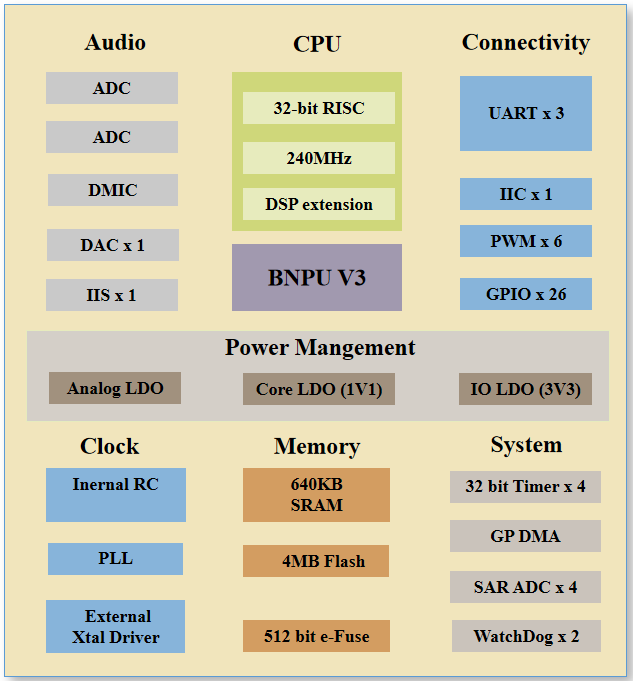
System Description
The system block diagram of the CI1306 chip is shown in Figure S-1. The chip includes multiple modules, including the brain neural network processor (BNPU). Each module is described below.
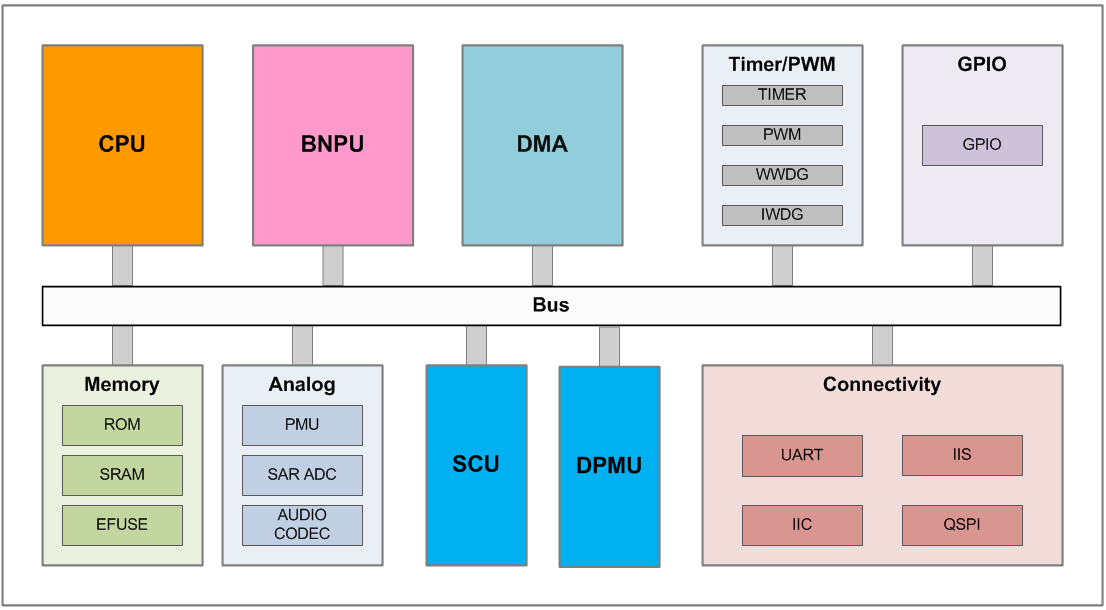
System Architecture
The chip system includes BNPU, CPU, ROM, SRAM, DMA, and various peripheral interfaces. Each functional module communicates and controls through the system bus supporting multi-core parallel processing architecture, as shown in Figure S-2.
Register Mapping
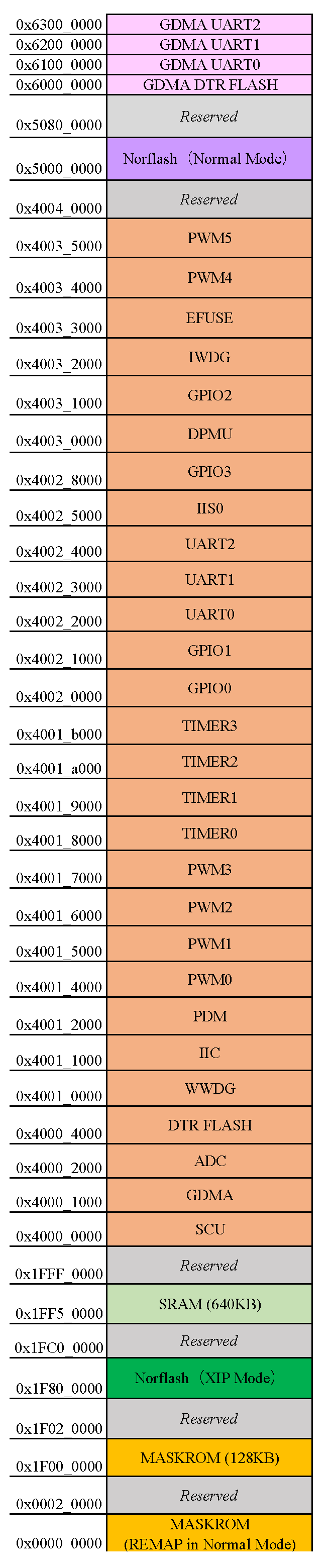
The chip register mapping is shown in Figure S-3. The internal ROM starts at address 0x00000000. SRAM starts at address 0x1FF00000 and spans to 0x1FF7FFFF, totaling 640KB. The remaining addresses are for peripheral interfaces.
Boot Mode Configuration
The chip has two startup modes: 1. ROM mode: Starts from internal ROM after power-on (normal operation mode) 2. SRAM mode: Starts from internal SRAM after power-on (debug mode)
The BOOT_SEL pin (multiplexed with PC5) selects the startup mode. During reset: - Set BOOT_SEL to 0 to start from ROM (mapped to 0x00000000) - Set BOOT_SEL to 1 to start from SRAM (requires pre-downloaded code)
In debug mode, SRAM maps to 0x00000000, allowing direct CPU access.
| Start mode selection pin (BOOT_SEL) power on level | Start mode | Description |
|---|---|---|
| 0 | ROM | Normal boot, internal ROM as boot area |
| 1 | SRAM | Debugging mode, with internal SRAM as the starting area |
Interrupt
With a built-in interrupt controller, the chip supports efficient interrupt handling. Key features include:
- Support software interrupt, timer interrupt and external interrupt;
- 32 programmable external interrupts;
- 3 bits interrupt priority configuration, that is, 8 priority levels;
- Support the software to dynamically and program matically modify the interrupt level and interrupt priority values;
- Support interrupt nesting based on interrupt level;
- Support fast vector interrupt processing mechanism;
- Support quick tail biting mechanism;
- NMI (Non Maskable Interrupt) is supported.
The interrupt vector table is shown below. When an interrupt occurs, the CPU executes instructions from the corresponding entry address.
Table S-2 Chip Interrupt Vector Table
| IRQ No. | Interrupt Source | Description |
|---|---|---|
| 0 | INT_WWDG | Window watchdog interrupt |
| 1 | INT_SCU | SCU interrupt |
| 2 | Reserved | Reserved |
| 3 | INT_ADC | ADC controller interrupt |
| 4 | Reserved | Reserved |
| 5 | INT_TIMER0 | Timer 0 interrupt |
| 6 | INT_TIMER1 | Timer 1 interrupt |
| 7 | INT_TIMER2 | Timer 2 interrupt |
| 8 | INT_TIMER3 | Timer 3 interrupt |
| 9 | INT_IIC | IIC interrupt |
| 10 | INT_GPIO0 | GPIO0 interrupt |
| 11 | INT_GPIO1 | GPIO1 interrupt |
| 12 | INT_UART0 | UART0 interrupt |
| 13 | INT_UART1 | UART1 interrupt |
| 14 | INT_UART2 | UART2 interrupt |
| 15 | INT_IIS0 | IIS0 interrupt |
| 16 | Reserved | Reserved |
| 17 | Reserved | Reserved |
| 18 | Reserved | Reserved |
| 19 | Reserved | Reserved |
| 20 | INT_PDM | PDM interrupt |
| 21 | INT_DTR | DTR Flash controller interrupt |
| 22 | Reserved | Reserved |
| 23 | INT_VDT | Low voltage detection indication interrupt |
| 24 | INT_EXT0 | External interrupt 0 |
| 25 | INT_EXT1 | External interrupt 1 |
| 26 | INT_IWDG | Independent watchdog interrupt |
| 27 | Reserved | Reserved |
| 28 | Reserved | Reserved |
| 29 | INT_EFUSE | EFUSE controller interrupt |
| 30 | INT_GPIO2 | GPIO2 interrupt |
Module Overview
This document details the frequently used modules and registers:
- System Control Unit (SCU)
- DMA
- Universal Timer and PWM Output
- Independent Watchdog (IWTD)
- Window Watchdog (WWTD)
- DTR_FLASH
- IIC
- IIS
- UART
- GPIO
- ADC
- EFUSE
The configuration and use of other modules, such as BNPU, CODEC, PDM, power management and PLL, EFUSE, have been included in the basic components provided by the CI130X SDK. It is not recommended that users directly modify the driver or directly operate the register to avoid abnormal operation of the basic components. It is recommended to directly use the standard driver interface provided in the CI130X SDK. If you really have special needs, please contact our technical support personnel for support.