ADC
Function Introduction
The chip integrates a 12-bit ADC with the following key features:
- 12-bit resolution
- Sampling rate up to 1 MSPS (15 cycles per conversion; a 15 MHz clock is required to achieve 1 MSPS)
- Six single-ended input channels. Only channel 5 is exposed; channels 0 and 1 are reserved for internal use. Other channels are unavailable.
- Operating current of 450 μA at 1 MSPS; shutdown current below 1 μA.
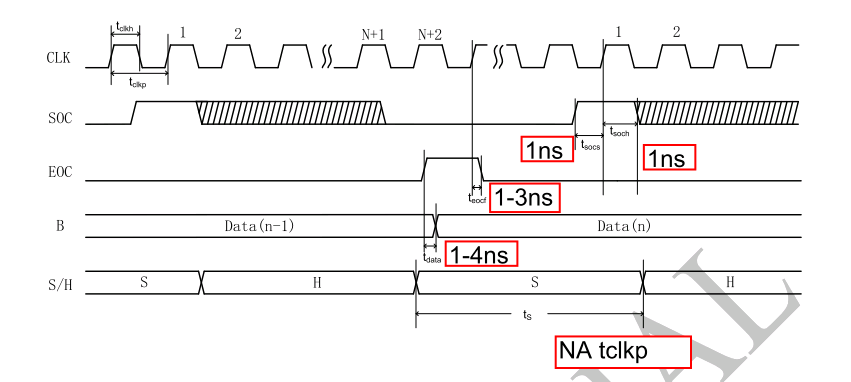
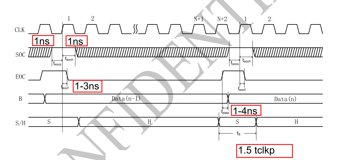
- Supports single-sample and continuous-sample modes. Timing diagrams are shown below.
Register Mapping
The base address of ADC register mapping is 0x40002000, and the specific register mapping is shown in Table A-1.
| Offset | Register | Width | Type | Reset Value | Description |
|---|---|---|---|---|---|
| 0x00 | ADCCTRL | 32 | R/W | 0x00000000 | ADC Control Register |
| 0x04 | ADCINTMASK | 16 | R/W | 0x0000 | ADC Interrupt Mask Register |
| 0x08 | ADCINTFLG | 16 | RO | 0x0000 | ADC Interrupt Flag Register |
| 0x0C | ADCINTCLR | 16 | WO | 0x0000 | ADC Interrupt Clear Register |
| 0x10 | ADCSOFTSOC | 16 | R/W | 0x0000 | ADC Software Trigger Register |
| 0x14 | ADCSOCCTRL | 32 | R/W | 0x00000000 | ADC Conversion Control Register |
| 0x18-0x24 | ADCRESULT2-ADCRESULT5 | 16 | R/W | 0x0000 | ADC Conversion Result Registers |
| 0x38 | CH0PERIOD | 16 | RO | 0x0000 | Channel 0 Sample Period |
| 0x3C | CH1PERIOD | 16 | R/W | 0x0000 | Channel 1 Sample Period |
| 0x40 | CH2PERIOD | 16 | R/W | 0x0000 | Channel 2 Sample Period |
| 0x44 | CH3PERIOD | 16 | R/W | 0x0000 | Channel 3 Sample Period |
| 0x48 | CH0MINVALUE | 16 | R/W | 0x0000 | Channel 0 Minimum Threshold |
| 0x4C | CH0MAXVALUE | 16 | R/W | 0x0FFF | Channel 0 Maximum Threshold |
| 0x50 | CH1MINVALUE | 16 | R/W | 0x0001 | Channel 1 Minimum Threshold |
| 0x54 | CH1MAXVALUE | 16 | R/W | 0x0FFF | Channel 1 Maximum Threshold |
| 0x58 | CH2MINVALUE | 16 | R/W | 0x0001 | Channel 2 Minimum Threshold |
| 0x5C | CH2MAXVALUE | 16 | R/W | 0x0FFF | Channel 2 Maximum Threshold |
| 0x60 | CH3MINVALUE | 16 | R/W | 0x0001 | Channel 3 Minimum Threshold |
| 0x64 | CH3MAXVALUE | 16 | R/W | 0x0FFF | Channel 3 Maximum Threshold |
| 0x68 | ADCSTAT | 16 | R | 0x0000 | ADC Status Register |
| 0x6C | ADCCTRLa | 32 | R/W | 0x00000000 | ADC Control Register A |
| 0x70 | ADCRSTN | 32 | R/W | 0x00000000 | ADC Reset Configuration Register |
| 0x74 | ADCOFFSET | 32 | R/W | 0x00000000 | ADC Offset Calibration Register |
| 0x78 | ADCLOADEN | 32 | R/W | 0x00000000 | ADC Load Enable Register |
| 0x7C | ADCPWRRDY | 32 | R/W | 0x00000000 | ADC Power Ready Register |
| 0x80 | CH4PERIOD | 16 | R/W | 0x0000 | Channel 4 Sample Period |
| 0x84 | CH5PERIOD | 16 | R/W | 0x0000 | Channel 5 Sample Period |
| 0x88 | CH4MINVALUE | 16 | R/W | 0x0000 | Channel 4 Minimum Threshold |
| 0x8C | CH4MAXVALUE | 16 | R/W | 0x0FFF | Channel 4 Maximum Threshold |
| 0x90 | CH5MINVALUE | 16 | R/W | 0x0000 | Channel 5 Minimum Threshold |
| 0x94 | CH5MAXVALUE | 16 | R/W | 0x0FFF | Channel 5 Maximum Threshold |
ADC Control Register (ADCCTRL)
Offset: 0x00
Reset value: 0x00000000
| Bit Field | Name | Reset Value | Type | Description |
|---|---|---|---|---|
| 31:24 | Reserved | 0x00 | R/W | Reserved |
| 23 | CH3MAXEN | 0 | R/W | CH3 Sampling Result Upper Threshold Interrupt Enable 0: Off 1: On |
| 22 | CH2MAXEN | 0 | R/W | CH2 sampling result threshold upper limit interrupt enable 0: off 1: on |
| 21 | CH1MAXEN | 0 | R/W | CH1 Sampling result threshold upper limit interrupt enable 0: Off 1: On |
| 20 | CH0MAXEN | 0 | R/W | CH0 upper limit of sampling result threshold interrupt enable 0: off 1: on |
| 19 | CH3MINEN | 0 | R/W | CH3 Sampling Result Threshold Lower Limit Interrupt Enable 0: Off 1: On |
| 18 | CH2MINEN | 0 | R/W | CH2 Sampling Result Threshold Lower Limit Interrupt Enable 0: Off 1: On |
| 17 | CH1MINEN | 0 | R/W | CH1 Sampling Result Threshold Lower Limit Interrupt Enable 0: Off 1: On |
| 16 | CH0MINEN | 0 | R/W | CH0 Sampling result threshold lower limit Interrupt enable 0: Off 1: On |
| 15: 13 | Reserved | 0x0 | R/W | Reserved |
| 12 | INTSEL | 0 | R/W | Interrupt generation condition selection 0: Interrupt request is generated at the end of each sampling 1: Interrupt request is generated when the sampling value is abnormal (exceeds the threshold value) This bit can only be configured as 1 when ADCCTRL [8] is configured as 1 in the monitoring mode |
| 11: 9 | Reserved | 0x0 | R/W | Reserved |
| 8 | PERIODEN | 0 | R/W | Periodic monitoring enable (can only work in single sampling mode) 0: Off 1: On |
| 7 | CH3EN | 0 | R/W | Channel 3 cycle monitoring enable 0: Off 1: On |
| 6 | CH2EN | 0 | R/W | Channel 2 cycle monitoring enable 0: OFF 1: ON |
| 5 | CH1EN | 0 | R/W | Channel 1 cycle monitoring enable 0: OFF 1: ON |
| 4 | CH0EN | 0 | R/W | Channel 0 cycle monitoring enable 0: Off 1: On |
| 2 | Reserved | 0 | R/W | Reserved |
| 1 | CONTEN | 0 | R/W | Continuous conversion enable 0: Single conversion mode 1: If SOCSOFT bit remains high, ADC will convert continuously |
| 0 | ADCEN | 0 | R/W | ADC circuit enable |
ADC Interrupt Mask Register (ADCINTMSK)
Offset: 0x04
Reset value: 0x0000
| Bit Field | Name | Reset Value | Type | Description |
|---|---|---|---|---|
| 15: 1 | Reserved | 0x0000 | R/W | Reserved |
| 0 | EOC_INT_EN | 0 | R/W | ADC interrupt mask bit 0: not masked 1: masked |
ADC Interrupt Flag Register (ADCINTFLG)
Offset: 0x08
Reset value: 0x0000
| Bit Field | Name | Reset Value | Type | Description |
|---|---|---|---|---|
| 15: 4 | Reserved | 0x000 | RO | Reserved |
| 3 | ADCFLG3 | 0 | RO | ADC channel 3 conversion completion interrupt flag bit, highly effective |
| 2 | ADCFLG2 | 0 | RO | ADC channel 2 conversion completion interrupt flag bit, highly effective |
| 1 | ADCFLG1 | 0 | RO | ADC channel 1 conversion completion interrupt flag bit, highly effective |
| 0 | ADCFLG0 | 0 | RO | ADC channel 0 conversion completion interrupt flag bit, highly effective |
ADC Interrupt Clear Register (ADCINTCLR)
Offset: 0x0C
Reset value: 0x0000
| Bit Field | Name | Reset Value | Type | Description |
|---|---|---|---|---|
| 15: 9 | Reserved | 0x00 | WO | Reserved |
| 8 | ADCINT_CLR | 0 | WO | Clear all channel interrupt flags, highly effective |
| 7: 4 | Reserved | 0x0 | WO | Reserved |
| 3 | ADCCLR3 | 0 | WO | ADC channel 3 conversion completion interrupt flag cleared, highly effective |
| 2 | ADCCLR2 | 0 | WO | ADC channel 2 conversion completion interrupt flag cleared, highly effective |
| 1 | ADCCLR1 | 0 | WO | ADC channel 1 conversion completion interrupt flag cleared, highly effective |
| 0 | ADCCLR0 | 0 | WO | ADC channel 0 conversion completion interrupt flag cleared, highly effective |
ADC Software Trigger Register (SOCSOFTCTRL)
Offset: 0x10
Reset value: 0x0000
| Bit Field | Name | Reset Value | Type | Description |
|---|---|---|---|---|
| 15: 1 | Reserved | 0x0000 | R/W | Reserved |
| 0 | SOCSOFT | 0 | R/W | ADC start conversion 0: no action 1: ADC start conversion |
ADC conversion control register (ADCSOCCTRL)
Offset: 0x14
Reset value: 0x00000000
| Bit Field | Name | Reset Value | Type | Description |
|---|---|---|---|---|
| 31:15 | Reserved | 0x00000 | R/W | Reserved |
| 14: 12 | SHTIME | 0x0 | R/W | Selection of sampling holding time: 0: SOC length is 1 AD_CLK cycle 1: SOC length is 2 AD_CLK cycle 2: SOC length is 3 AD_CLK cycle 3: SOC length is 4 AD_CLK cycle 4: SOC length is 5 AD_CLK cycle other:invalid value |
| 11: 8 | Reserved | 0x0 | R/W | Reserved |
| 7: 5 | CHSEL | 0x0 | R/W | Conversion channel selection 0: ADC_IN0 1:ADC_IN1 2:ADC_IN2 3:ADC_IN3 |
| 4: 0 | Reserved | 0x00 | R/W | Reserved |
ADC conversion result register (ADCRESULTx)
Offset: 0x18-0x24
Reset value: 0x0000
| Bit Field | Name | Reset Value | Type | Description |
|---|---|---|---|---|
| 15: 12 | Reserved | 0x0 | R/W | Reserved |
| 11: 0 | ADCOUT | 0x000 | R/W | ADC conversion result |
Note: x=2,3,4,5, ADCRESULTx corresponds to the conversion result of channel x respectively
Channel 0 Sample Period Register (CH0PERIOD)
Offset: 0x38
Reset value: 0x0000
| Bit Field | Name | Reset Value | Type | Description |
|---|---|---|---|---|
| 15: 0 | CH0PERIOD | 0x0000 | R/W | Channel 0 Sampling period: (CH0PERIOD+1) * 512 |
Channel 1 Sampling Period Register (CH1PERIOD)
Offset: 0x3C
Reset value: 0x0000
| Bit Field | Name | Reset Value | Type | Description |
|---|---|---|---|---|
| 15: 0 | CH1PERIOD | 0x0000 | R/W | Channel 1 Sampling period: (CH1PERIOD+1) * 512 |
Channel 2 Sample Period Register (CH2PERIOD)
Offset: 0x40
Reset value: 0x0000
| Bit Field | Name | Reset Value | Type | Description |
|---|---|---|---|---|
| 15: 0 | CH2PERIOD | 0x0000 | R/W | Channel 2 Sampling period: (CH2PERIOD+1) * 512 |
Channel 3 Sample Period Register (CH3PERIOD)
Offset: 0x44
Reset value: 0x0000
| Bit Field | Name | Reset Value | Type | Description |
|---|---|---|---|---|
| 15: 0 | CH3PERIOD | 0x0000 | R/W | Channel 3 Sampling period: (CH3PERIOD+1) * 512 |
Channel 0 Lower Threshold Register (CH0MINVALUE)
Offset: 0x48
Reset value: 0x0000
| Bit Field | Name | Reset Value | Type | Description |
|---|---|---|---|---|
| 15: 0 | MINVALUE | 0x0000 | R/W | Lower threshold of channel 0 |
Channel 0 upper threshold register (CH0MAXVALUE)
Offset: 0x4C
Reset value: 0x0FFF
| Bit Field | Name | Reset Value | Type | Description |
|---|---|---|---|---|
| 15: 0 | MAXVALUE | 0x0FFF | R/W | Upper threshold of channel 0 |
Channel 1 lower threshold register (CH1MINVALUE)
Offset: 0x50
Reset value: 0x0001
| Bit Field | Name | Reset Value | Type | Description |
|---|---|---|---|---|
| 15: 0 | MINVALUE | 0x0001 | R/W | Lower threshold of channel 1 |
Channel 1 upper threshold register (CH1MAXVALUE)
Offset: 0x54
Reset value: 0x0FFF
| Bit Field | Name | Reset Value | Type | Description |
|---|---|---|---|---|
| 15: 0 | MAXVALUE | 0x0FFF | R/W | Upper threshold of channel 1 |
Channel 2 Lower Threshold Register (CH2MINVALUE)
Offset: 0x58
Reset value: 0x0001
| Bit Field | Name | Reset Value | Type | Description |
|---|---|---|---|---|
| 15:00 | MINVALUE | 0x0001 | R/W | Lower threshold of channel 2 |
Channel 2 upper threshold register (CH2MAXVALUE)
Offset: 0x5C
Reset value: 0x0FFF
| Bit Field | Name | Reset Value | Type | Description |
|---|---|---|---|---|
| 15: 0 | MAXVALUE | 0x0FFF | R/W | Upper threshold of channel 2 |
Channel 3 lower threshold register (CH3MINVALUE)
Offset: 0x60
Reset value: 0x0000
| Bit Field | Name | Reset Value | Type | Description |
|---|---|---|---|---|
| 15: 0 | MINVALUE | 0x0001 | R/W | Lower threshold of channel 3 |
Channel 3 upper threshold register (CH3MAXVALUE)
Offset: 0x64
Reset value: 0x0FFF
| Bit Field | Name | Reset Value | Type | Description |
|---|---|---|---|---|
| 15: 0 | MAXVALUE | 0x0FFF | R/W | Upper threshold of channel 3 |
ADC Status Register (ADCSTAT)
Offset: 0x68
Reset value: 0x0000
| Bit Field | Name | Reset Value | Type | Description |
|---|---|---|---|---|
| 15: 1 | Reserved | 0x0000 | RO | Reserved |
| 0 | PRDBSY | 0 | RO | Current ADC working status 0: ADC conversion completed, idle status 1: ADC working |
ADC control register a (ADCCTRLa)
Offset: 0x6C
Reset value: 0x00000000
| Bit Field | Name | Reset Value | Type | Description |
|---|---|---|---|---|
| 31:10 | Reserved | 0x0000 | R/W | Reserved |
| 9 | CH5MAXEN | 0 | R/W | CH5 Sampling Result Threshold Lower Limit Interrupt Enable 0: Off 1: On |
| 8 | CH4MAXEN | 0 | R/W | CH4 Sampling Result Threshold Lower Limit Interrupt Enable 0: Off 1: On |
| 7 | CH5MINEN | 0 | R/W | CH5 Sampling Result Threshold Lower Limit Interrupt Enable 0: Off 1: On |
| 6 | CH4MINEN | 0 | R/W | CH4 Sampling Result Threshold Lower Limit Interrupt Enable 0: Off 1: On |
| 5 | CH5EN | 0 | R/W | Channel 5 cycle monitoring enable 0: OFF 1: ON |
| 4 | CH4EN | 0 | R/W | Channel 4 cycle monitoring enable 0: Off 1: On |
| 3 | RSTN | 0 | R/W | ADC reset function 0: Start reset 1: Normal mode |
| 2 | SDIF | 0 | R/W | Analog sampling signal mode selection 0: Single ended mode 1: Differential mode, which is used in offset calibration mode |
| 1 | Reserved | 0x0000 | R/W | Reserved |
| 0 | DISH | 0 | R/W | Normal mode and offset calibration selection 0: Normal mode 1: Offset calibration mode |
Note 1: ADC is reset by default after power on. To use it, you must first set the RSTN bit to 1. At the same time, the ADC module has timing requirements when it is powered on and needs to keep the reset signal for a period of time after startup. Therefore, the following reset configuration register is added. When this configuration is 0, the RSTN signal is released after 6 ADC CLK cycles after the ADCEN signal is valid. When configured to other values, the RSTN signal is released after the configured value plus 6 ADC CLK cycles after the ADCEN signal is valid, so as to ensure normal ADC function
Note 2: ADC adds the offset calibration function to adapt to individual errors caused by chip production or environment. When using, set DISH and SDIF to 1 to short-circuit the internal VIP and VIN signals. At this time, calculate the difference between the sampling value read by the channel port corresponding to the ADC and the ideal conversion value 800H, use the difference as the offset value for calibration, and write it to the OFFSET bit of the ADC offset calibration register. Note that the value of this bit has a complement. If the value of this bit is set to 2F, 2F is the complement of - 17. At this time, when ADC sets DISH and SDIF to 0 and returns to the normal working mode, the sampling value will automatically calculate and subtract 17; If the value of this bit is set to 1A, 1A is the complement of 26. At this time, when ADC sets DISH and SDIF to 0 and returns to the normal working mode, the sampling value will be automatically calculated plus 26
ADC reset configuration register (ADCRSTN)
Offset: 0x70
Reset value: 0x00000000
| Bit Field | Name | Reset Value | Type | Description |
|---|---|---|---|---|
| 31:6 | Reserved | 0x0000 | R/W | Reserved |
| 5: 0 | ADCRSTN | 0 | R/W | Reset signal increases the number of cycles that remain low after the ADCEN signal is enabled |
ADC Offset Calibration Register (ADCOFFSET)
Offset: 0x74
Reset value: 0x00000000
| Bit Field | Name | Reset Value | Type | Description |
|---|---|---|---|---|
| 31:6 | Reserved | 0x0000 | R/W | Reserved |
| 5: 0 | OFFSET | 0 | R/W | Set ADC offset calibration value |
ADC Load Register (ADCLOADEN)
Offset: 0x78
Reset value: 0x00000000
| Bit Field | Name | Reset Value | Type | Description |
|---|---|---|---|---|
| 31:1 | Reserved | 0x0000 | R/W | Reserved |
| 0 | LOADEN | 0 | R/W | Enable loading signal, write 1 to load, and self clear after loading |
Note: This register needs to be configured with LOADEN bit as 0 before the ADC module is successfully reset to normal function, and the value of the register will take effect, and then the set EN_ADC of the ADCCTRL control register as 1, start ADC module to work
ADC Reset Status Register (ADCPWRRDY)
Offset: 0x7C
Reset value: 0x00000000
| Bit Field | Name | Reset Value | Type | Description |
|---|---|---|---|---|
| 31:1 | Reserved | 0x0000 | R | Reserved |
| 0 | PWRRDY | 0 | R | ADC reset release flag, highly effective |
Channel 4 Sample Period Register (CH4PERIOD)
Offset: 0x80
Reset value: 0x0000
| Bit Field | Name | Reset Value | Type | Description |
|---|---|---|---|---|
| 15: 0 | CH4PERIOD | 0x0000 | R/W | Channel 4 Sampling period: (CH4PERIOD+1) * 512 |
Channel 5 Sample Period Register (CH5PERIOD)
Offset: 0x84
Reset value: 0x0000
| Bit Field | Name | Reset Value | Type | Description |
|---|---|---|---|---|
| 15:00 | CH5PERIOD | 0x0000 | R/W | Channel 5 sampling period: (CH5PERIOD+1) * 512 |
Channel 4 Lower Threshold Register (CH4MINVALUE)
Offset: 0x88
Reset value: 0x0000
| Bit Field | Name | Reset Value | Type | Description |
|---|---|---|---|---|
| 15: 12 | Reserved | 0x0 | R | Reserved |
| 11:0 | MINVALUE | 0x000 | R/W | Lower threshold of channel 4 |
Channel 4 upper threshold register (CH4MAXVALUE)
Offset: 0x8C
Reset value: 0x0FFF
| Bit Field | Name | Reset Value | Type | Description |
|---|---|---|---|---|
| 15: 12 | Reserved | 0x0 | R | Reserved |
| 11: 0 | MAXVALUE | 0xFFF | R/W | Upper threshold of channel 4 |
Channel 5 lower threshold register (CH5MINVALUE)
Offset: 0x90
Reset value: 0x0000
| Bit Field | Name | Reset Value | Type | Description |
|---|---|---|---|---|
| 15: 12 | Reserved | 0x0 | R | Reserved |
| 11: 0 | MINVALUE | 0x000 | R/W | Lower threshold of channel 5 |
Channel 5 upper threshold register (CH5MAXVALUE)
Offset: 0x94
Reset value: 0x0FFF
| Bit Field | Name | Reset Value | Type | Description |
|---|---|---|---|---|
| 15: 12 | Reserved | 0x0 | R | Reserved |
| 11: 0 | MAXVALUE | 0xFFF | R/W | Upper threshold of channel 5 |