Hardware Design
The CI1301, CI1302, and CI1303 chips require only a few external components to support various voice applications. For the voice processing, the chip supports both single microphone differential input and single-ended input, with optional AEC (Acoustic Echo Cancellation) functionality. Users can select appropriate circuits based on design requirements for functionality, power consumption, and cost. Below is a detailed description of the simplest application reference circuit for this chip.
Application Reference Diagram
The application reference diagram is shown in Figure H-1, using the CI1303 as an example (the pin and circuit connections are identical for CI1301, CI1302, and CI1303).
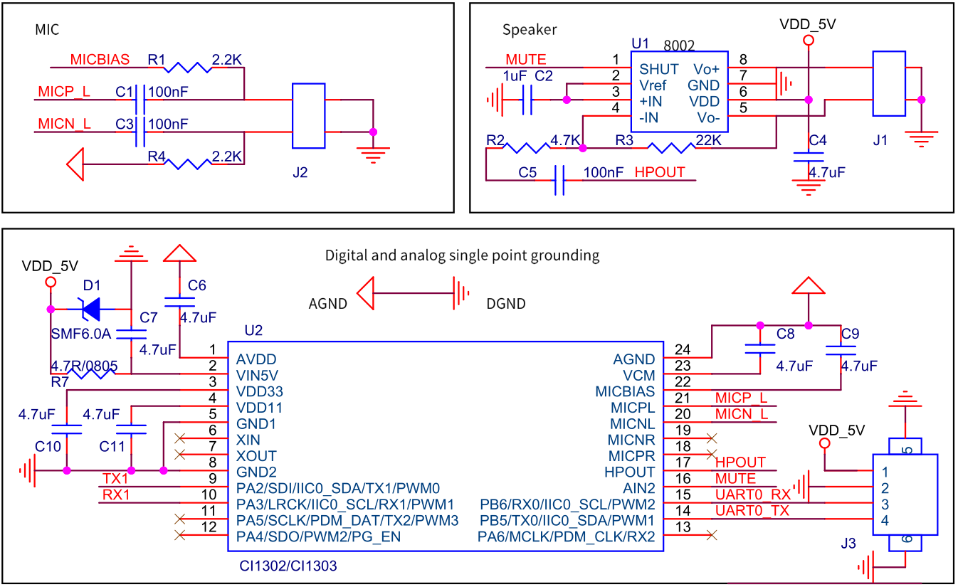
The diagram above shows the simplest application circuit for CI1303 supporting single microphone differential input and amplifier output. The chip can be powered directly with 5V, and users can design according to the specifications of the external components shown in the diagram.
If the board-level online upgrade function is to be considered during schematic design, the UART0 pin can be led out to facilitate Firmware Update of the flash in the main chip through UART0 after PCB board placement is completed. The PA4 (PG_EN) pin of the chip is internally pulled up. The power-on defaults to the upgrade mode. After power-on, the upgrade signal sent from the external UART0 port should be detected. If there is one, the upgrade should be started directly. Extended by adding detection of upgrade mode, the default boot time of the chip is about 850mS; If the user has high requirements for the boot time, the PA4 pin can be led out, two 2.2K Ω pull-down resistors can be added to the ground, and a test point can be added between the two 2.2K Ω resistors. At this time, the chip is powered on in the normal mode, and the boot time is about 350mS, which can shorten the boot time. If you want to upgrade online at this time, you can externally supply high level to the intermediate test points connected by two 2.2K Ω resistors, pull up the PA4 pin, and then upgrade through UART0.
Applications with this chip can select differential microphone design or single-ended microphone design, and the differential microphone design in the above figure is recommended. If the user has requirements for cost, the microphone part in the above figure can be modified to a single-ended microphone design, which can use fewer passive devices than the differential microphone. However, this method is only recommended for applications where the microphone line length is less than 20 cm, otherwise the speech recognition effect will not be as good as the differential microphone design because the line length is too long and the anti-interference effect is not enough. The power amplifier shown in the figure above is a Class AB amplifier, with the 8002 power amplifier chip recommended in the diagram. Users may select alternative power amplifier chips based on their specific solution requirements. If the power amplifier function is not required, this circuit section can be omitted to reduce costs. For applications requiring AEC, users can utilize a microphone input channel to connect the AEC analog signal input.
If the user has no special requirements for the power consumption of the solution, it is recommended to directly use the PMU inside the chip for power supply. If there is a power consumption requirement, the external DCDC chip can be added to power the chip 1.1V to reduce the power consumption. All UART ports of the chip support 5V communication. The UART0 port in the above figure is a 3.3V signal. If 5V is to be connected, add a pull-up resistor connected to 5V around the RX and TX pins of UART0. No additional voltage conversion circuit is required.
Chipintelli provides a variety of solution reference schematics, which can meet most common application scenarios. In the actual application development, the customer needs to carefully select one of the most suitable reference schematics for reference and design optimization according to the specific product functional performance requirements, system characteristics, and application scenarios. As Chipintelli is unable to master all product systems and application knowledge, customers or solution partners are expected to fully test and verify product functional performance (including the matching of voice chips and modules with product systems) in combination with product systems and application scenarios before mass production. If there are unclear and uncertain problems during the design modification process, please contact Chipintelli FAE engineer for full communication. The list of reference schematics is as follows:
| Solution name | Solution function | Solution application scenario | Document center link |
|---|---|---|---|
| Typical solution | Single microphone differential microphone input with echo cancellation function | Suitable for widely used products, products with broadcasting and echo cancellation | ☞Reference schematic for typical solution |
| Low power consumption solution | 1.1V power supply is powered by external DCDC, significantly reducing power consumption | Products with high requirements for power consumption, such as products with energy consumption level restrictions | ☞Reference schematic for low power consumption solution |
| Highly reliable solution | Strong ESD EMC anti-interference ability, power interference resistance ability, improve product reliability | For products with poor system power quality, high requirements for product reliability, products requiring FCC CE certification, and products with high requirements for ESD, | ☞Reference schematic of high reliability solution |
| Low cost solution | Single ended microphone, the simplest circuit without AEC application | Products with extreme cost requirements and low reliability requirements, products with microphone line length less than 20cm, such as toys and FMCG products | ☞Reference schematic for low cost solution |
| Double mic solution | double mic differential input, without AEC function | Products with double mic enhancement, sound source positioning, and high noise resistance requirements | ☞Reference schematic of double mic solution |
| External AEC solution | Single microphone AEC supports external broadcast and echo cancellation function | Applications that need to eliminate external broadcast, such as massage chair application external Bluetooth broadcast can use this solution | ☞External AEC solution Reference schematic |
| Battery solution | Functions of battery power supply, charging and discharging, switching control, etc. | Battery powered intelligent voice products, such as voice toys, voice remote controllers, intelligent voice personal wearable products, etc | ☞Reference schematic for battery solution |
| Light control lighting solution | AC-DC power circuit, thyristor control, zero crossing detection, external DCDC power supply | Light control lighting products, such as ceiling lamp, desk lamp, floor light, etc. |
The schematic source document and PCB reference can be found in the ☞Chipintelli AI Speech Development Platform.
PCB Layout Design
Power Circuit
-
Power Wiring
Power input should include overvoltage and surge protection. For 5V input, use TVS devices and 4.7 Ω resistors. Route the wiring through TVS first, then through resistors to the chip. Power supply trace widths should be at least 15mil for 3.3V and 1.2V supplies. Use copper clad traces where possible, keeping them short and thick. The narrowest power supply trace width must be at least 8mil to prevent closed loops -
Power Decoupling Capacitor
The power decoupling capacitor is arranged close to the corresponding pin.
Electrostatic Protection Requirements
In the design of two-layer boards, try to route in the TOP layer to maintain the integrity of the BOTTOM ground plane. If ESD devices are designed, try to close the ESD devices to the pins of the plug-in to improve the protection effect.
Other Considerations for Application
- Due to the semiconductor technology principle, the RC oscillator built in the chip will produce a certain temperature drift in high and low temperature environments. If the operating temperature range of the user’s application scenario is - 40 to 85 ℃, it is recommended that the external crystal oscillator be used as the circuit solution. In addition, if the application scenario requires high-precision PWM output (the frequency accuracy error is required to be less than ± 2%) or high-speed serial communication (the baud rate is greater than 115200bps), it is also recommended to directly use the external crystal oscillator.
- For applications operating between -10°C to 70°C with low-speed serial communication (baud rate ≤ 115200bps), the internal RC oscillator may be used (with a frequency tolerance of ±1.5%). To minimize communication errors when using the internal oscillator, Chipintelli offers a baud rate adaptation solution. This requires implementing a handshake protocol where the host device must respond within 50ms of receiving the handshake command. With this adaptation, the operational temperature range can be extended to -20°C to 85°C.
- If the application scenario does not require the frequency accuracy of the RC oscillator, the RC oscillator built in the chip can be directly used.
- The chip includes a Power Management Unit (PMU) with multiple LDOs that generate 3.3V and 1.1V supplies. The external 5V power supply must maintain ripple below 300mV. For applications with stringent RF performance or power consumption requirements, consider using separate external power supplies.
- The chip is manufactured using lead-free processes. During SMT assembly, adhere to lead-free reflow profile specifications for temperature and time parameters.
- Handle all components using proper ESD precautions. Use anti-static packaging and grounding when storing and transporting chips to prevent electrostatic discharge damage.
- CI1303 chip supports high-capacity neural network model, has better noise reduction effect and supports OTA upgrade function. CI1303 and CI1302 chips support OTA upgrade function, CI1301 do not support OTA upgrade function.