DPMU
The DPMU (Digital Power Management Unit) handles analog PMU control, clock gating, resets, PLL configuration, system wake-up events, and IO pin multiplexing. Paired with the SCU (System Control Unit), it manages the chip’s core clock and power infrastructure. Since the analog subsystem is critical to reliable operation, it is not recommended that users configure it by themselves—use the SDK’s default settings. This document excludes analog PMU register details and focuses solely on reset, clock gating, and IO multiplexing registers.
DPMU Register Mapping
The DPMU registers base address is 0x40030000. See Table DPMU-1 for register offsets and descriptions.
| Offset | Name | Bit Width | Type | Reset Value | Description |
|---|---|---|---|---|---|
| 0x00 | CFG_LOCK_CFG | 32 | R/W | 0x00000000 | Configuration lock register |
| 0x10 | SYS_RESET_CFG | 32 | R/W | 0x00,000,000 | System reset configuration register |
| 0x14 | SYS_SOFTRST_CFG | 32 | R/W | 0x00000000 | System software reset configuration register |
| 0x20 | SYS_CLK_SEL_CFG | 32 | R/W | 0x00000004 | System clock selection configuration register |
| 0x30 | PLL_CFG | 32 | R/W | 0x00001407 | PLL configuration register |
| 0x34 | AON_CLK_PARAM_CFG | 32 | R/W | 0x00204080 | Clock frequency division configuration register |
| 0x40 | AON_CLK_PARAM_EN_CFG | 32 | R/W | 0x00000000 | Clock division enable configuration register |
| 0x50 | AON_CLKGATE_CFG | 32 | R/W | 0x0000007F | Clock gating configuration register |
| 0x70 | AON_RESET_CFG | 32 | R/W | 0x0000001F | Reset configuration register |
| 0x140 | IOREUSE_CFG0 | 32 | R/W | 0x00000000 | IO multiplexing configuration register 0 |
| 0x144 | IOREUSE_CFG1 | 32 | R/W | 0x00000000 | IO multiplexing configuration register 1 |
| 0x14C | OD_CFG0 | 32 | R/W | 0x00000000 | IO open drain status configuration register 0 |
| 0x150 | PD_CFG0 | 32 | R/W | 0x00000000 | IO pull-down status configuration register 0 |
| 0x158 | PU_CFG0 | 32 | R/W | 0x00000000 | IO pull-up status configuration register 0 |
| 0x160 | DS_CFG0 | 32 | R/W | 0x00000000 | IO drive capacity configuration register 0 |
| 0x164 | DS_CFG1 | 32 | R/W | 0x00000000 | IO drive capability configuration register 1 |
| 0x190 | AD_CFG0 | 32 | R/W | 0x00000000 | IO multiplexing AD configuration register 0 |
| 0x194 | OD_CFG1 | 32 | R/W | 0x00000000 | IO open drain status configuration register 1 |
| 0x198 | PD_CFG1 | 32 | R/W | 0x00000000 | IO pull-down status configuration register 1 |
| 0x19C | PU_CFG1 | 32 | R/W | 0x00000000 | IO pull-up status configuration register 1 |
| 0x1A0 | DS_CFG2 | 32 | R/W | 0x00000000 | IO drive capability configuration register 2 |
| 0x1C0 | RST_STATE_REG | 32 | R/W | 0x00000001 | Reset status register |
Configure Lock Register (CFG_LOCK_CFG)
Offset: 0x00
Reset value: 0x00000000
| Bit Field | Name | Reset Value | Type | Description |
|---|---|---|---|---|
| 31:0 | CFG_LOCK_CFG | 0x00000000 | R/W | Register LOCK command. When the software configures other registers, it needs to write 0x51AC0FFE to this register first to unlock it. When reading this register: 1: unlocked, can be written 0: It is not unlocked and cannot be written. |
System Reset Configuration Register (SYS_RESET_CFG)
Offset: 0x10
Reset value: 0x00000000
| Bit Field | Name | Reset Value | Type | Description |
|---|---|---|---|---|
| 31:10 | Reserved | 0 | R/W | Reserved |
| 9:8 | wwdg_rst_sel | 0 | R/W | Reset range when WWDG module detects abnormal dog feeding: 2’b10: reset the whole system (PLL CPU peripherals SCU internal clock divider is reset) 2’b11: reset the system bus (CPU peripherals SCU internal clock divider is reset) other value: no reset operation |
| 7:6 | iwdg_rst_sel | 0 | R/W | Reset range when the IWDG module detects abnormal dog feeding: 2’b10: reset the whole system (PLL CPU peripherals SCU internal clock divider is reset) 2’b11: reset the system bus (CPU peripherals SCU internal clock divider is reset) other value: no reset operation |
| 5:4 | soft_rst_sel | 0 | R/W | Reset range of software reset: 2’b10: reset the whole system (PLL CPU peripherals SCU internal clock divider is reset) 2’b11: reset the system bus (CPU peripherals SCU internal clock divider is reset) other value: no reset operation |
| 3:2 | Reserved | 0 | R/W | Reserved |
| 1:0 | cpu_rstreq_rst_sel | 0 | R/W | Reset range when the CPU core sends a reset request: 2’b10: reset the CPU core 2’b11: reset the system bus (CPU peripherals SCU internal clock divider is reset) other value: no reset operation |
System Software Reset Configuration Register (SYS_SOFTRST_CFG)
Offset: 0x14
Reset value: 0x00000000
| Bit Field | Name | Reset Value | Type | Description |
|---|---|---|---|---|
| 31:0 | SOFT_SOFTRST_CFG | 0 | R/W | To provide a software operable system reset mode, set this register. When the software write parameter matches the fixed characteristic value 0xdeadbeef, a software reset request is generated |
System Clock Selection Configuration Register (SYS_CLK_SEL_CFG)
Offset: 0x20
Reset value: 0x00000004
| Bit Field | Name | Reset Value | Type | Description |
|---|---|---|---|---|
| 31:3 | Reserved | 0 | R/W | Reserved |
| 2 | sys_clk_sel | 0x1 | R/W | System clock selection: 0: System SRC clock is used. The clock source is determined by the 1:0 bit configuration of this register 1: Clock generated by PLL |
| 1:0 | src_clk_sel | 0 | R/W | System SRC clock source selection: 2’b01: clock generated by internal RC oscillator 2’b11: clock generated by external crystal oscillator other: Reserved |
PLL Configuration Register (PLL_CFG)
Offset: 0x30
Reset value: 0x00,001,407
| Bit Field | Name | Reset Value | Type | Description |
|---|---|---|---|---|
| 31:15 | Reserved | 0 | R/W | Reserved |
| 14 | BYPASS | 0x0 | R/W | PLL clock bypass enable: 0: output the clock after PLL processing (frequency multiplication, frequency division) 1: output the clock before PLL processing |
| 13: 6 | M | 0x50 | R/W | PLL coefficient M |
| 5: 2 | N | 0x1 | R/W | PLL coefficient N |
| 1:0 | OD | 0x3 | R/W | PLL coefficient OD |
PLL frequency multiplication can be calculated according to the following formula: PLL clock=input clock × Value of M/Value of N × 1/NO Where NO=2 to the power of (OD value)
Clock Division Configuration Register (AON_CLK_PARAM_CFG)
Offset: 0x34
Reset value: 0x00204080
| Bit Field | Name | Reset Value | Type | Description |
|---|---|---|---|---|
| 31:24 | Reserved | 0 | R/W | Reserved |
| 23:17 | timer_pwm_div | 0x10 | R/W | Clock division coefficient of TIMER and PWM modules |
| 16:10 | iwdg_div | 0x10 | R/W | IWDG module clock division factor |
| 9:6 | apb_div | 0x2 | R/W | APB bus clock division coefficient, which affects all peripherals on the APB bus |
| 5:0 | ipcore_div | 0x0 | R/W | IP core clock division factor |
Clock Division Enable Configuration Register (AON_CLK_PARAM_EN_CFG)
Offset: 0x40
Reset value: 0x00000000
| Bit Field | Name | Reset Value | Type | Description |
|---|---|---|---|---|
| 31:5 | Reserved | 0 | R/W | Reserved |
| 4 | timer_gpwm_div_en | 0x0 | R/W | TIMER and PWM module clock division coefficient update enable: 0: Do not update 1: Update After this bit is configured as 1 and takes effect, it is automatically cleared to 0 |
| 3 | iwdg_div_en | 0x0 | R/W | IWDG module clock division factor update enable: 0: Do not update 1: Update After this bit is configured as 1 and takes effect, it is automatically cleared to 0 |
| 2 | apb_div_en | 0x0 | R/W | APB bus clock division factor update enable: 0: Do not update 1: Update After this bit is configured as 1 and takes effect, it is automatically cleared to 0 |
| 1 | ipcore_div_en | 0x0 | R/W | IP kernel clock division factor update enable: 0: Do not update 1: Update After this bit is configured as 1 and takes effect, it is automatically cleared to 0 |
| 0 | pll_cfg_en | 0x0 | R/W | PLL configuration update enable: 0: Do not update 1: Update After this bit is configured as 1 and takes effect, it is automatically cleared to 0 |
Clock Gating Configuration Register (AON_CLKGATE_CFG)
Offset: 0x50
Reset value: 0x0000007F
| Bit Field | Name | Reset Value | Type | Description |
|---|---|---|---|---|
| 31:6 | Reserved | 0x3 | R/W | Reserved |
| 5 | iwdg_cpu_halt_cken | 0x1 | R/W | IWDG module clock gating enable when the CPU is in the halt state: 0: automatically turn off the clock 1: do not automatically turn off the clock |
| 4 | timer1_gpwm1_cken | 0x1 | R/W | TIMER1 and PWM1 module clock gating enable: 0: close clock 1: open clock |
| 3 | timer0_gpwm0_cken | 0x1 | R/W | TIMER0 and PWM0 module clock gating enable: 0: close clock 1: open clock |
| 2 | efuse_cken | 0x1 | R/W | EFUSE module clock gating enable: 0: close clock 1: open clock |
| 1 | iwdg_cken | 0x1 | R/W | IWDG module clock gating enable: 0: close clock 1: open clock |
| 0 | gpio_cken | 0x1 | R/W | GPIO module clock gating enable: 0: close clock 1: open clock |
Reset Configuration Register (AON_RESET_CFG)
Offset: 0x70
Reset value: 0x0000001F
| Bit Field | Name | Reset Value | Type | Description |
|---|---|---|---|---|
| 31:5 | Reserved | 0x3 | R/W | Reserved |
| 4 | pll_rsten | 0x1 | R/W | PLL module reset enable: 0: reset 1: no reset |
| 3 | timer01_gpwm01_rsten | 0x1 | R/W | TIMER0/1 and PWM0/1 module reset enable: 0: reset 1: not reset |
| 2 | efuse_rsten | 0x1 | R/W | EFUSE module reset enable: 0: reset 1: not reset |
| 1 | iwdg_rsten | 0x1 | R/W | IWDG module reset enable: 0: reset 1: not reset |
| 0 | gpio_rsten | 0x1 | R/W | GPIO module reset enable: 0: reset 1: not reset |
The following is an IO related register set. The specific usage method will be described after listing all the registers
IO Multiplexing Configuration Register 0 (IOREUSE_CFG0)
Offset: 0x140
Reset value: 0x00000000
| Bit Field | Name | Reset Value | Type | Description |
|---|---|---|---|---|
| 31 | Reserved | 0 | R/W | Reserved |
| 30:0 | IOREUSE_CFG0 | 0x0 | R/W | IOREUSE_For CFG0 configuration items, please refer to the following descriptions and tables for specific functions |
IO Multiplexing Configuration Register 1 (IOREUSE_CFG1)
Offset: 0x144
Reset value: 0x00000000
| Bit Field | Name | Reset Value | Type | Description |
|---|---|---|---|---|
| 31:21 | Reserved | 0 | R/W | Reserved |
| 20:0 | IOREUSE_CFG1 | 0x0 | R/W | IOREUSE_For CFG1 configuration item, please refer to the following description and table for specific functions |
IO Open Drain Status Configuration Register 0 (OD_CFG0)
Offset: 0x14C
Reset value: 0x00000000
| Bit Field | Name | Reset Value | Type | Description |
|---|---|---|---|---|
| 31:15 | Reserved | 0 | R/W | Reserved |
| 14:0 | OD_CFG0 | 0x0 | R/W | OD_For CFG0 configuration items, please refer to the following descriptions and tables for specific functions |
IO Pull-Down Status Configuration Register 0 (PD_CFG0)
Offset: 0x150
Reset value: 0x00000000
| Bit Field | Name | Reset Value | Type | Description |
|---|---|---|---|---|
| 31 | Reserved | 0 | R/W | Reserved |
| 30:0 | PD_CFG0 | 0x0 | R/W | PD_For CFG0 configuration items, please refer to the following descriptions and tables for specific functions |
IO Pull-Up Status Configuration Register 0 (PU_CFG0)
Offset: 0x158
Reset value: 0x00000000
| Bit Field | Name | Reset Value | Type | Description |
|---|---|---|---|---|
| 31 | Reserved | 0 | R/W | Reserved |
| 30:0 | PU_CFG0 | 0x0 | R/W | PU_For CFG0 configuration items, please refer to the following descriptions and tables for specific functions |
IO Drive Capability Configuration Register 0 (DS_CFG0)
Offset: 0x160
Reset value: 0x00000000
| Bit Field | Name | Reset Value | Type | Description |
|---|---|---|---|---|
| 31:0 | DS_CFG0 | 0x0 | R/W | DS_For CFG0 configuration items, please refer to the following descriptions and tables for specific functions |
IO Drive Capability Configuration Register 1 (DS_CFG1)
Offset: 0x164
Reset value: 0x00000000
| Bit Field | Name | Reset Value | Type | Description |
|---|---|---|---|---|
| 31:0 | DS_CFG1 | 0x0 | R/W | DS_For CFG1 configuration item, please refer to the following description and table for specific functions |
IO Multiplexing AD Configuration Register 0 (AD_CFG0)
Offset: 0x190
Reset value: 0x00000003
| Bit Field | Name | Reset Value | Type | Description |
|---|---|---|---|---|
| 31:12 | Reserved | 0 | R/W | Reserved |
| 11:0 | AD_CFG0 | 0x3 | R/W | AD_For CFG0 configuration items, please refer to the following descriptions and tables for specific functions |
IO Open Drain Status Configuration Register 1 (OD_CFG1)
Offset: 0x194
Reset value: 0x00000000
| Bit Field | Name | Reset Value | Type | Description |
|---|---|---|---|---|
| 31:16 | Reserved | 0 | R/W | Reserved |
| 15:0 | OD_CFG1 | 0x0 | R/W | OD_For CFG1 configuration item, please refer to the following description and table for specific functions |
IO Pull-Down Status Configuration Register 1 (PD_CFG1)
Offset: 0x198
Reset value: 0x00000000
| Bit Field | Name | Reset Value | Type | Description |
|---|---|---|---|---|
| 31:16 | Reserved | 0 | R/W | Reserved |
| 15:0 | PD_CFG0 | 0x0 | R/W | PD_For CFG0 configuration items, please refer to the following descriptions and tables for specific functions |
IO Pull-Up Status Configuration Register 1 (PU_CFG1)
Offset: 0x19C
Reset value: 0x00000000
| Bit Field | Name | Reset Value | Type | Description |
|---|---|---|---|---|
| 31:16 | Reserved | 0 | R/W | Reserved |
| 15:0 | PU_CFG1 | 0x0 | R/W | PU_For CFG1 configuration item, please refer to the following description and table for specific functions |
IO Drive Capability Configuration Register 2 (DS_CFG2)
Offset: 0x1A0
Reset value: 0x00000000
| Bit Field | Name | Reset Value | Type | Description |
|---|---|---|---|---|
| 31:0 | DS_CFG2 | 0x0 | R/W | DS_Refer to the following description and table for specific functions of CFG2 configuration item |
Each bit of the above IO related register group is valid when it is configured as 1. IO multiplexing determines the functional status of the corresponding IO. AD multiplexing determines whether the corresponding IO is configured as an analog ADC input port. Pull up and pull down and open drain registers determine whether the corresponding IO is enabled in internal pull up, pull down or open drain status (external 5V input is supported when IO is open drain). DS registers determine the driving ability of the corresponding IO. There are two valid data bits, When the temperature is 25 ° C and the chip operates at 3.3V and 1.1V, the DS value and corresponding nominal drive capacity are shown in the following table:
| DS | Ioh (output current at high level 2.4V) | Iol (input current at low level 2.4V) |
|---|---|---|
| 0 | 33.1mA | 19.3mA |
| 1 | 39.7mA | 23.1mA |
| 2 | 46.4mA | 26.9mA |
| 3 | 53mA | 30.8mA |
The control relationship table of each IO and corresponding IO configuration register of the chip is shown in the figure below:
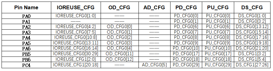
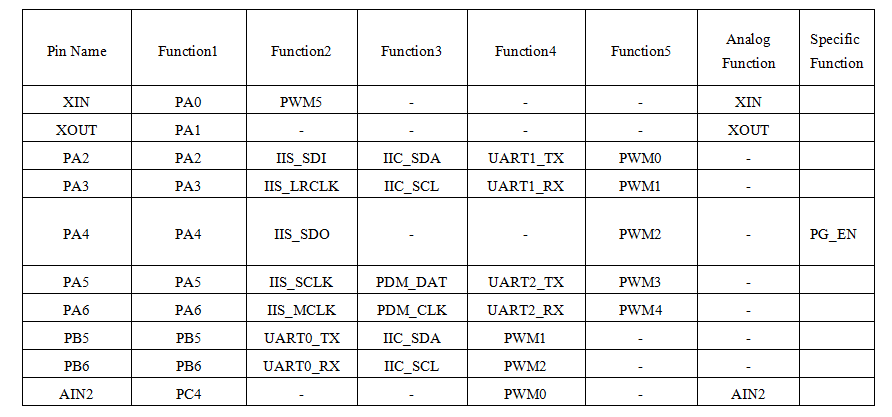
In the above IO multiplexing configuration, the value of the IOREUSE register bit of the IO configuration determines the current operating mode of the IO. The relationship between the operating mode and IO is shown in the following figure:
Reset Status Register (RST_STATE_REG)
Offset: 0x1C0
Reset value: 0x00000001
| Bit Field | Name | Reset Value | Type | Description |
|---|---|---|---|---|
| 31:6 | Reserved | 0 | W1C | Reserved |
| 5 | SOFT_RST_STATE | 0x0 | W1C | The software causes the reset status bit. 1 is the reset status, and this bit is cleared to 0 when writing 1 |
| 4 | WWDG_RST_STATE | 0x0 | W1C | The reset status bit caused by WWDG. 1 is the reset status, and this bit is cleared to 0 when writing 1 |
| 3 | IWDG_RST_STATE | 0x0 | W1C | Status bit reset caused by IWDG. 1 is reset status, and this bit is cleared to 0 when writing 1 |
| 2 | Reserved | 0 | W1C | Reserved |
| 1 | CPU_REQ_RST_STATE | 0x0 | W1C | The reset status bit caused by the CPU reset request. 1 is the reset status, and this bit is cleared to 0 when writing 1 |
| 1 | POWER_ON_RST_STATE | 0x1 | W1C | Status bit reset due to power on, 1 is reset status, and this bit is cleared to 0 when writing 1 |