Pin Description
The CI1306 chip pin diagram is shown in Figure P-1:
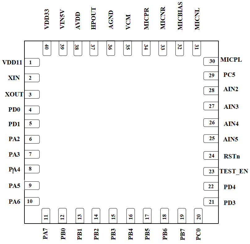
The functions of each pin of the chip are described in the following table:
| Pin Number | Pin name | Pin type | IO 5V-Tolerant | IO power-on default state | Description and alternate functions |
|---|---|---|---|---|---|
| 1 | VDD11 | P | - | - | 1.1V output or 1.1V Power supply, output apacitance/input capacitance is 4.7uF |
| 2 | XIN | I | - | - | 1. XIN (external crystal and oscillator interface, initial state at startup, no external crystal oscillator is required for normal application) 2. GPIO PA0 3. PWM5 |
| 3 | XOUT | O | - | - | 1. XOUT(external crystal and oscillator interface, initial state at startup, no external crystal oscillator is required for normal application) 2. GPIO PA1 |
| 4 | PD0 | IO | √ | IN,T+D | GPIO PD0 |
| 5 | PD1 | IO | √ | IN,T+D | GPIO PD1 |
| 6 | PA2 | IO | √ | IN,T+D | 1. GPIO PA2(Initial state at startup) 2. IIS_SDI 3. IIC_SDA 4. UART1_TX 5. PWM0 |
| 7 | PA3 | IO | √ | IN,T+D | 1. GPIO PA3(Initial state at startup) 2. IIS_LRCLK 3. IIC_SCL 4. UART1_RX1 5. PWM1 |
| 8 | PA4 | IO | √ | IN,T+U | 1. GPIO PA4(Initial state at startup)/PG_EN(Note1) 2. IIS_SDO 3. PWM2 |
| 9 | PA5 | IO | √ | IN,T+D | 1. GPIO PA5(Initial state at startup) 2. IIS_SCLK 3. PDM_DAT 4. UART2_TX 5. PWM3 |
| 10 | PA6 | IO | √ | IN,T+D | 1. GPIO PA6(Initial state at startup) 2. IIS_MCLK 3. PDM_CLK 4. UART2_RX 5. PWM4 |
| 11 | PA7 | IO | √ | IN,T+D | 1. GPIO PA7(Initial state at startup) 2. PWM0 3. UART1_TX 4. EXT_INT[0] |
| 12 | PB0 | IO | √ | IN,T+D | 1. GPIO PB0(Initial state at startup) 2. PWM1 3. UART1_RX 4. EXT_INT[1] |
| 13 | PB1 | IO | √ | IN,T+D | 1. GPIO PB1(Initial state at startup) 2. PWM2 3. UART2_TX |
| 14 | PB2 | IO | √ | IN,T+D | 1. GPIO PB2(Initial state at startup) 2. PWM3 3. UART2_RX |
| 15 | PB3 | IO | √ | IN,T+D | 1. GPIO PB3(Initial state at startup) 2. PWM4 3. IIC_SDA |
| 16 | PB4 | IO | √ | IN,T+D | 1. GPIO PB4(Initial state at startup) 2. PWM5 3. IIC_SCL |
| 17 | PB5 | IO | √ | IN,T+U | 1. GPIO PB5(Initial state at startup) 2. UART0_TX 3. IIC_SDA 4. PWM1 |
| 18 | PB6 | IO | √ | IN,T+U | 1. GPIO PB6(Initial state at startup) 2. UART0_RX 3. IIC_SCL 4. PWM2 |
| 19 | PB7 | IO | √ | IN,T+U | 1. GPIO PB7(Initial state at startup) 2. UART1_TX 3. IIC_SDA 4. PWM3 |
| 20 | PC0 | IO | √ | IN,T+U | 1. GPIO PC0(Initial state at startup) 2. UART1_RX 3. IIC_SCL 4. PWM4 |
| 21 | PD3 | IO | - | IN,T+D | GPIO PD3 |
| 22 | PD4 | IO | - | IN,T+D | GPIO PD4 |
| 23 | TEST_EN | I | - | - | TEST Pin (Note2) |
| 24 | RSTn | I | - | - | Reset Pin ( Note3) |
| 25 | AIN5 | IO | - | IN,T+D | 1. GPIO PC1(Initial state at startup) 2. UART2_TX 3. PWM3 4. PDM_DAT 5. ADC input channel 5 |
| 26 | AIN4 | IO | - | IN,T+U | 1. GPIO PC2(Initial state at startup) 2. UART2_RX 3. PWM2 4. PDM_CLK 5. ADC input channel 4 |
| 27 | AIN3 | IO | - | IN,T+D | 1. GPIO PC3(Initial state at startup) 2. IIC_SDA 3. PWM1 4. PDM_DAT 5. ADC input channel 3 |
| 28 | AIN2 | IO | - | IN,T+U | 1. GPIO PC4(Initial state at startup) 2. IIC_SCL 3. PWM0 4. PDM_CLK 5. ADC input channel 2 |
| 29 | PC5 | IO | √ | IN,T+D | GPIO PC5/BOOT_SEL (Note4) |
| 30 | MICPL | I | - | - | Left Microphone P input |
| 31 | MICNL | I | - | - | Left Microphone N input |
| 32 | MICBIAS | O | - | - | Microphone bias output |
| 33 | MICNR | I | - | - | Right Microphone N input |
| 34 | MICPR | I | - | - | Right Microphone P input |
| 35 | VCM | O | - | - | VCM Output |
| 36 | AGND | P | - | - | Analog ground |
| 37 | HPOUT | O | - | - | DAC output |
| 38 | AVDD | P | - | - | 3.3V output or 3.3V analog power supply, output capacitance/input capacitance is 4.7uF |
| 39 | VIN5V | P | - | - | VIN5V is the PMU power supply input pin. The normal working input voltage range is 3.6V-5.5V. A 4.7uf input capacitor is connected externally. The maximum input voltage of this pin is 6.5V. Note that overvoltage and surge protection devices need to be added, such as a TVS and a 4.7 Ω resistor to protect against surge impact |
| 40 | VDD33 | P | - | - | 3.3V output, output capacitance/input capacitance is 4.7uF |
| 41 | GND | P | - | - | Ground PAD (Note5) |
The status of IO pin in the above table is defined as follows:
I Input
O Output
IO Bidirectional
P Power or ground
T+D Tri-state positive pull-down
T+U Tri-state positive pull-up
OUT Power on defaults to output mode
IN Power on defaults to input mode
All IO support drive capacity can be configured, and the up and down resistance can be configured.
Note 1: PA4 (PG_EN) pin judges whether to program according to the level state at power on, and starts the programming function at high power level
Note 2: TEST_EN is the enable test function pin, which is pulled down internally. When the pin is powered on, the input level of the pin is detected. The chip starts normally at low level and enters the test mode at high level
Note 3: RSTn is an external reset input pin. When the pull down time is greater than 100uS, the chip can be reset
Note 4: BOOT_SEL pin judges the entry device started by the system according to the level state at power on, starting from Flash at low power level and starting from SRAM at high power level
Note 5: There is a heat dissipation pad at the bottom of the QFN40 package, which needs to be grounded during use