Hardware Design
The CI1324X chip requires minimal external components to develop end-product solutions supporting various intelligent voice applications. This chip supports single microphone with either differential or single-ended input. The application design can be tailored based on functional requirements, power consumption, cost, and other factors to select the most suitable circuit design solution.
Using the CI13242 typical application as an example, the following outlines the key points and considerations for application design:
Reference Application Circuit
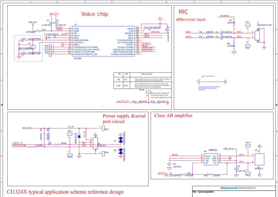
The above diagram shows the reference design circuit for a typical application of the CI1324X series chips (including CI13242), featuring single microphone differential input and power amplifier output. This design is not limited to any specific end product. Application designs should be based on the principle of compatibility with host terminal products. For reference schematics and PCB layouts tailored to your product’s functional and performance requirements, please visit the Chipintelli Documentation Center and AI Platform: https://document.Chipintelli.com/.
When designing the application solution, if board-level upgrade functionality is required, the UART0 pins can be brought out via connectors or test points to facilitate firmware programming or upgrades through UART0 after PCB assembly.
The PA4 (PG_EN) pin of CI13242 has an internal 3.3V pull-up resistor. During power-on, the system checks if this pin is pulled to 3.3V high level. If high and an upgrade signal is detected on the UART0 pins, the system enters upgrade mode. If an external pull-down resistor to ground is connected, the chip can skip the upgrade mode detection and directly enter normal boot mode for faster startup. For applications requiring fast startup, the PA4 pin can be brought out with two 2.2KΩ pull-down resistors in series to ground, with a test point between them (for specific implementation, refer to the reference schematic or consult our FAE). In this configuration, the system boots in normal mode with a startup time of approximately 350ms. For in-circuit upgrades, applying 3.3V to the test point between the two 2.2KΩ resistors will pull the PA4 pin high, enabling UART0-based upgrades. The two operating modes of PG_EN are shown in the table below:
| PG_EN External Resistor Diagram | R5\R6 Installation | PG_EN Level | Boot Time |
|---|---|---|---|
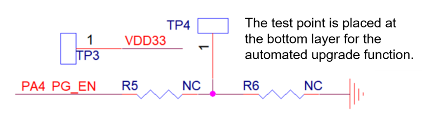 |
R5\R6 Not Installed | High, Upgrade Mode | 850ms |
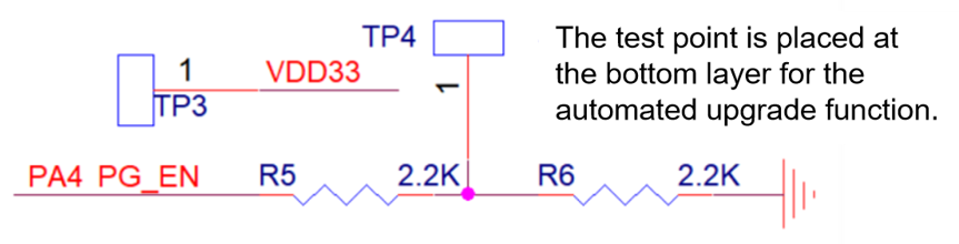 |
R5\R6 = 2.2KΩ | Low, Normal Mode | 350ms |
CI13242 supports both differential and single-ended microphone inputs, with the differential microphone design shown in Figure H-1 being recommended. For cost-sensitive designs, a single-ended microphone input can be used to reduce component count on the microphone input line. However, this approach is only recommended when the microphone input line length is less than 20cm, as longer lines may compromise noise immunity and degrade voice recognition performance.
The typical application features a Class AB power amplifier, with the 8002 series being recommended. The amplifier circuit can be omitted to reduce costs if voice playback functionality is not required.
For applications without ultra-low power requirements, it is recommended to use the internal PMU of CI13242 for power supply to minimize costs. For ultra-low power applications, an external DCDC circuit can be used to supply 1.1V to the CI13242 to reduce system power consumption.
All UART ports on CI13242 support 5V level communication. The UART0 port in the diagram uses 3.3V level communication as an example. For 5V level communication, simply add 5V pull-up resistors to the UART0 RX and TX pins; no level-shifting circuit is required.
PCB Layout Design
Power Circuit
Power Traces
Implement overvoltage and surge protection for power input by including TVS devices and 4.7Ω resistors on the 5V input. Route the power traces through the TVS first, then through the resistor to the chip. The trace width should be determined by the actual current requirements: minimum 15 mil for 3.3V power traces and 15 mil for 1.1V power traces. Use copper pour where possible, keep power traces short and wide, maintain a minimum width of 8 mil at the narrowest point, and avoid creating closed loops in power traces.
Power Decoupling Capacitors
Place power decoupling capacitors as close as possible to their corresponding pins.
ESD Protection Requirements
For two-layer board designs, route traces primarily on the TOP layer to maintain the integrity of the BOTTOM ground plane. When ESD protection devices are used, position them as close as possible to the connector pins for optimal protection.
Additional Application Notes
-
CI1324X is manufactured using lead-free, environmentally friendly materials. When performing SMT soldering, please set the reflow temperature and time parameters according to lead-free standards. A typical SMT soldering temperature profile is shown below:
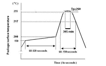 Figure H-2 Chip SMT Soldering Temperature Profile
 -
Proper ESD precautions must be taken during handling, transportation, and processing of CI1324X. Use ESD-safe packaging materials at all times.
-
The chip has a Moisture Sensitivity Level (MSL) rating of 3. Store the device under MSL3 conditions before use. If the package has been exposed to ambient conditions for longer than the MSL3 specification allows, bake the device before SMT soldering.