Pin Diagram and Functional Description
Pin Diagram
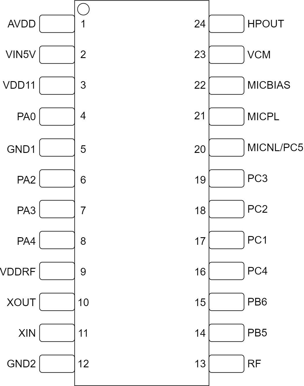
Pin Description
| Pin No. | Pin Name | Type | 5V Tolerant | Default State | Pin Function |
|---|---|---|---|---|---|
| 1 | AVDD | P | - | - | ● Internal LDO-3.3V output ● 3.3V power supply input for analog circuits (Note1) |
| 2 | VIN5V | P | - | - | ● Power supply voltage input, range 3.6V to 5.5V (Note1) |
| 3 | VDD11 | P | - | - | ● LDO-1.1V output ● 1.1V core power supply input (Note1) |
| 4 | PA0 | IO | - | - | ● XIN (default power-on state) ● GPIO PA0 ● PWM2 |
| 5 | GND1 | P | - | - | ● Ground |
| 6 | PA2 | IO | √ | IN,T+D | ● GPIO PA2 (default power-on state) ● I2C_SDA ● PWM0 ● PWMP |
| 7 | PA3 | IO | √ | IN,T+D | ● GPIO PA3 (default power-on state) ● I2C_SCL ● PWM1 ● PWMN |
| 8 | PA4 | IO | √ | IN,T+U | ● GPIO PA4 (default power-on state) ● PG_EN (Note2) ● PWM2 ● PWMP |
| 9 | VDDRF | P | - | - | ● RF power supply input (Note1) |
| 10 | XOUT | IO | - | - | ● Crystal oscillator output (Note4) |
| 11 | XIN | IO | - | - | ● Crystal oscillator input (Note4) |
| 12 | GND2 | P | - | - | ● Ground |
| 13 | RF | IO | - | - | ● RF antenna |
| 14 | PB5 | IO | √ | IN,T+U | ● GPIO PB5 (default power-on state) ● UART0_TX ● I2C_SDA ● PWM1 ● PWMP |
| 15 | PB6 | IO | √ | IN,T+U | ● GPIO PB6 (default power-on state) ● UART0_RX ● I2C_SCL ● PWM2 ● PWMN |
| 16 | PC4 | IO | - | IN,T+U | ● Reserved (default power-on state) ● PC4 ● SCL ● PWM0 |
| 17 | PC1 | IO | - | IN,T+D | ● Reserved (default power-on state) ● PC1 ● TX2 ● PWM3 |
| 18 | PC2 | IO | - | IN,T+U | ● Reserved (default power-on state) ● PC2 ● RX2 ● PWM2 |
| 19 | PC3 | IO | - | IN,T+D | ● Reserved (default power-on state) ● PC3 ● SDA ● PWM1 |
| 20 | MICN/PC5 | IO | - | IN,T+D | ● Microphone N input ● Reserved (default power-on state) ● PC5 ● BOOT (Note3) |
| 21 | MICP | I | - | - | ● Microphone P input |
| 22 | MICBIAS | O | - | - | ● Microphone bias output |
| 23 | VCM | O | - | - | ● VCM Output |
| 24 | HPOUT | O | - | - | ● DAC output |
Note1: External 4.7uF capacitor required for this pin
Note2: System enters programming mode if this pin is high during power-on
Note3: Do not pull up this pin during power-on, otherwise the system will enter debug mode
Note4: Pin10 XOUT and Pin11 XIN are Bluetooth crystal I/O pins, providing clock for Bluetooth only; Voice clock is provided by the internal RC oscillator
Symbol Definitions
I Input
O Output
IO Bidirectional
P Power or Ground
T+D Tri-state with pull-down
T+U Tri-state with pull-up
OUT Default to output mode on power-up
IN Default to input mode on power-up
All IOs support configurable drive strength and pull-up/down resistors.
Multiplexed Functions
| Pin Number | Function1 | Function2 | Function3 | Function4 | Function5 | Function6 | Specific Function |
|---|---|---|---|---|---|---|---|
| PA0 | PA0 | PWM2 | - | - | - | - | XIN |
| PA2 | PA2 | - | I2C_SDA | - | PWM0 | PWMP | - |
| PA3 | PA3 | - | I2C_SCL | - | PWM1 | PWMN | - |
| PA4 | PA4 | - | - | - | PWM2 | - | PG_EN(Note5) |
| PB5 | PB5 | UART0_TX | I2C_SDA | PWM1 | PWMP | - | - |
| PB6 | PB6 | UART0_RX | I2C_SCL | PWM2 | PWMN | - | - |
| PC1 | - | PC1 | TX2 | PWM3 | - | - | - |
| PC2 | - | PC2 | RX2 | PWM2 | - | - | - |
| PC3 | - | PC3 | SDA | PWM1 | - | - | - |
| PC4 | - | PC4 | SCL | PWM0 | - | - | - |
| PC5 | - | PC5 | - | - | - | - | BOOT(Note3) |
Note3: Do not pull up this pin during power-on, otherwise the system will enter debug mode.
Note5: The PA4 (PG_EN) pin has an internal pull-up by default. If the system detects a high level on this pin during power-up and there is a Firmware Update signal on the UART0 interface, it will automatically enter upgrade mode, allowing programming of the internal Flash via the upgrade tool. If no Firmware Update signal is detected on the UART0 interface or if the PA4 pin voltage is low, the system will enter normal operation mode.