CI-F24XGS01S Module Datasheet
Module Introduction
Overview
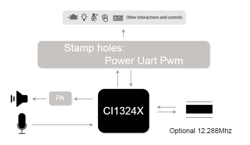
The CI-F24XGS01S is a versatile, high-performance, and cost-effective low-power offline voice recognition module, with the main chip options of CI13241 or CI13242. The module’s application design is simple and convenient, as shown in the following application diagram.
The CI-F24XGS01S module has the following main features:
-
Excellent Recognition Performance: Supports offline neural network computing, single-microphone noise reduction enhancement, single-microphone echo cancellation, 360° omnidirectional sound pickup, and can suppress environmental noise to ensure voice recognition accuracy in noisy environments. The offline voice recognition does not rely on network, with low latency, high performance, and recognition rate of over 97%. The response time for recognition at a distance of up to 10 meters can reach 0.2 seconds.
-
Compact Design: Module dimensions are 18x20mm (LxW), featuring a stamp hole and pin header design for convenient reflow soldering and pin soldering.
-
Minimal Component Count: The entire solution requires only an audio power amplifier chip and a few passive components in addition to the voice recognition chip to achieve full functionality.
-
Simple External Interface: Two 5V power supply inputs, two UART communication interfaces, one microphone interface, one speaker interface, and four GPIO interfaces.
-
Wide Operating Voltage Range: 3.6V-5V.
-
Low Power Consumption: Suitable for products with high energy efficiency requirements or battery-powered applications.
-
High Reliability Design: All BOM components are industrial-grade.
-
Flexible Model Selection: The module can be configured with either CI13241 or CI13242 chips based on the required number of command entries, as shown in the following table:
| Number of Entries | Up to 100 Command Entries | 100-300 Command Entries |
|---|---|---|
| Corresponding Voice Chip Model | CI13241 | CI13242 |
| Corresponding Module Model | CI-F241GS01S | CI-F242GS01S |
Note: The module can be used with a matching function baseboard. For more information about the function baseboard, please click: ☞CI-B02-MB Development Kit Instructions
Main Chip Introduction
CI13241 and CI13242 are dedicated artificial intelligence chips for voice processing, supporting offline voice recognition in both Chinese and English. They are widely used in household appliances, lighting, toys, wearable devices, industrial, automotive, and other product fields to achieve voice interaction, control, and various intelligent voice solutions.
CI13241&CI13242 integrate Chipintelli’s self-developed next-generation Brain Neural Processing Unit (BNPU V3.5) and CPU core, with a system frequency up to 210MHz. They feature 288KByte of built-in SRAM, PMU power management unit, RC oscillator, high-performance low-power Audio Codec, and multiple peripheral control interfaces including UART, I2C, I2S, PWM, GPIO, and PDM. The chips require only a few external components such as resistors and capacitors to implement various intelligent voice product hardware solutions, offering excellent cost performance.
For more detailed information about CI13241&CI13242 chips, please click the following link:
☞CI13241&CI13242 Chip Datasheet
Module Application Scenarios
The CI-F24XGS01S module can be used as a combination solution of voice recognition front-end + terminal product main control board (as shown in the figure below), or as the main control module for products such as lighting fixtures and toys.
The CI-F24XGS01S module supports up to 300 offline voice recognition commands and can be applied to various terminal products with relatively complex control requirements, such as smart air conditioners, smart fans, heating tables, clothes dryers, small household appliances, toys, and lighting.

Module Specifications
Physical Layout
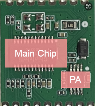
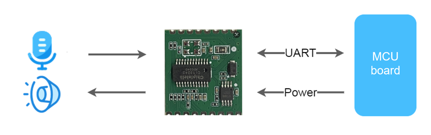
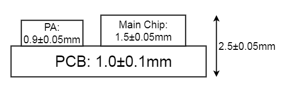
The physical diagram of the CI-F24XGS01S module is shown in Figure 4. The module features single-sided surface mounting, with main functional components including the voice recognition chip (CI13241/CI13242) and audio power amplifier. The basic workflow is as follows: voice commands are input through the microphone, processed by the voice recognition IC for voice recognition and command processing, and then the corresponding electrical signal commands are output through the serial port while being played back through the audio power amplifier and speaker. The audio power amplifier configured in this module has a maximum driving power of 1.5W@8Ω.
Note: The physical diagram is for illustration purposes only. The silkscreen on the surface of components may vary between different batches of modules, but this will not affect the module’s performance. The actual module status shall prevail.
Module Dimensions
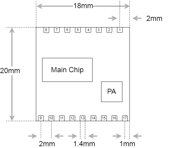
The CI-F24XGS01S module dimensions are shown in Figure 5. The module’s structure and dimensions can be used for related structural design.
CI-F24XGS01S module structure and dimensions related data are shown in Figure 5. When developing applications, the structure and dimensions of the module can be used for related structural design.
Module Hardware Interface Definition
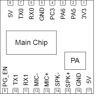
CI-F24XGS01S module has the following functional interfaces:
- Single microphone interface, module application design requires microphone socket or soldering point design on the bottom board, ESD devices need to be configured on the microphone line. To ensure good voice recognition performance, it is recommended to use a microphone with a sensitivity of -32±3dB and a signal-to-noise ratio of ≥65dB, please click ☞Reference Microphone Components to learn more information;
- Single speaker interface, module application design requires speaker socket or soldering point design on the bottom board, to ensure good voice playback effect, it is recommended to use a cavity speaker, please click ☞Reference Speaker Components to learn more information;
- Two UART interfaces of the module: UART0 interface is used for module Firmware Update, UART1 interface is used for serial port communication with the main controller MCU; The four GPIO interfaces of the module can be used as ordinary GPIO interfaces, or can be reused as PWM interfaces, used for light control and infrared control signal transmission.
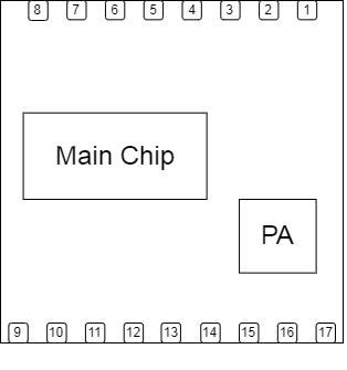
The pin function definition of the module is shown in Table 2:
| Pin Number | Pin Name | Pin Type | IO Drive Capability | IO Default State | Function Definition |
|---|---|---|---|---|---|
| 1 | 3.3V | P | - | - | 3.3V power output, Note1 |
| 2 | PA5 | IO | √ | IN,T+D | 1.GPIO PA5 2.IIS_SCLK 3.UART2_TX 4.PWM channel 3 5.PDM_DAT |
| 3 | PA6 | IO | √ | IN,T+D | 1.GPIO PA6 2.IIS_MCLK 3.UART2_RX 4.PWMN0 |
| 4 | PC3 | IO | √ | IN,T+D | 1. GPIO PC3 2.SDA 3.PWM channel 1 |
| 5 | GND | P | - | - | GND |
| 6 | RX0 | IO | √ | IN,T+U | 1. GPIO PB6 2.UART0_RX 3.IIC_SCL 4.PWM channel 2 |
| 7 | TX0 | IO | √ | IN,T+U | 1. GPIO PB5 2.UART0_TX 3.IIC_SDA 4.PWM channel 1 |
| 8 | 5V | P | - | - | 5V power |
| 9 | PG_EN | IO | √ | IN,T+D | 1.GPIO PA4/PG_EN.Note2 2.IIS_SDO 3.PWM channel 2 |
| 10 | TX1 | IO | √ | IN,T+D | 1.GPIO PA2 2.IIS_SDI 3.IIC_SDA 4.UART1_TX 5.PWM channel 0 |
| 11 | RX1 | IO | √ | IN,T+D | 1.GPIO PA3 2.IIS_LRCLK 3.IIC_SCL 4.UART1_RX 5.PWM channel 1 |
| 12 | MICL- | - | - | - | Microphone negative |
| 13 | MICL+ | - | - | - | Microphone positive |
| 14 | SKPL- | - | - | - | Speaker output |
| 15 | SKPL+ | - | - | - | Speaker output |
| 16 | GND | P | - | - | GND |
| 17 | 5V | P | - | - | 5V power |
Note1:3.3v output current does not exceed 10mA.
Note2:PG_EN pin determines whether to program based on the pin level when powered on, high level starts programming function.
The annotation symbols in the table are defined as follows:
I input
O output
IO bidirectional
P power or ground
T+D tristate plus pull-down
T+U tristate plus pull-up
OUT power-on defaults to output mode
Module Electrical Characteristics Parameters
| Parameter | Minimum Value | Typical Value | Maximum Value | Unit | Remarks |
|---|---|---|---|---|---|
| Module working voltage | / | 3.6 | 5 | 5.5 | V |
| Module playback current (normal volume) | 4 Ω 3W speaker | / | 65 | / | mA |
| Module working current | / | / | 35 | / | mA |
| Quiet listening state current | 5V power supply | / | 25 | / | mA |
| Module IO interface voltage | / | 3 | 3.3 | 5 | V |
NOTE1:5V is the typical supply voltage for the module. Input voltage exceeding 5.5V may damage the module.
NOTE2:Module playback current can reach 250mA, in principle, a power supply with 500mA driving capability (twice the margin) is required for the module.
NOTE3:Typical value is tested in mute state. The maximum value is tested during recognition and playback state.
Module Electrical Characteristics Parameters
| Parameter | Minimum Value | Typical Value | Maximum Value | Unit | Remarks |
|---|---|---|---|---|---|
| Module working environment temperature | -40 | 25 | 85 | °C | / |
| Module storage environment temperature | -40 | 25 | 100 | °C | / |
| Module storage humidity | 0% | / | 5% | RH | / |
Module Application
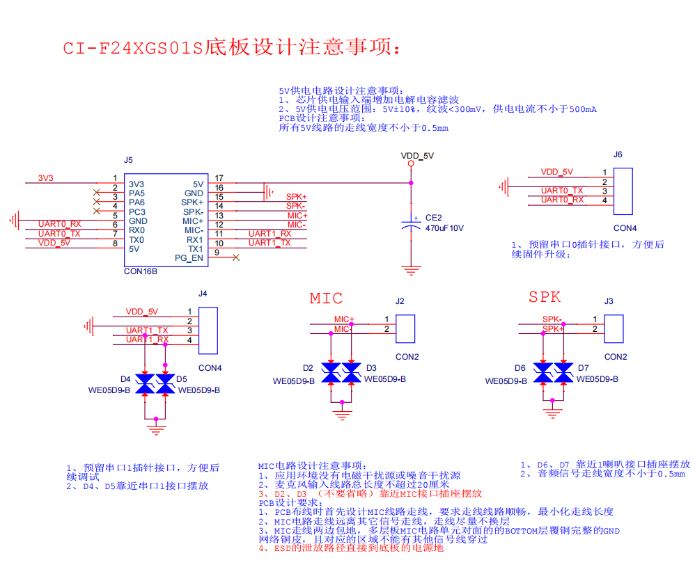
Module Baseboard Design Reference
To use this module, a corresponding debug baseboard or host motherboard is required. The main functions of the debug baseboard are to carry this module, provide the required operating voltage, microphone and speaker interfaces, and communicate with the module.
-
It is recommended to place a large-capacity filter capacitor near the module’s power input pins to ensure the stability of the 5V input voltage. The larger the power supply ripple or noise of the 5V input, the larger the capacitance of this filter capacitor needs to be.
-
Configure ESD protection devices near the speaker and microphone sockets to ensure the module’s electrostatic protection capability.
-
Reserve UART external pin headers on the baseboard to facilitate subsequent module upgrades and debugging.
-
The four GPIO interfaces can be multiplexed as PWM interfaces for light control.
The reference design of the module baseboard is shown in the figure below.
Module Power-on and Startup
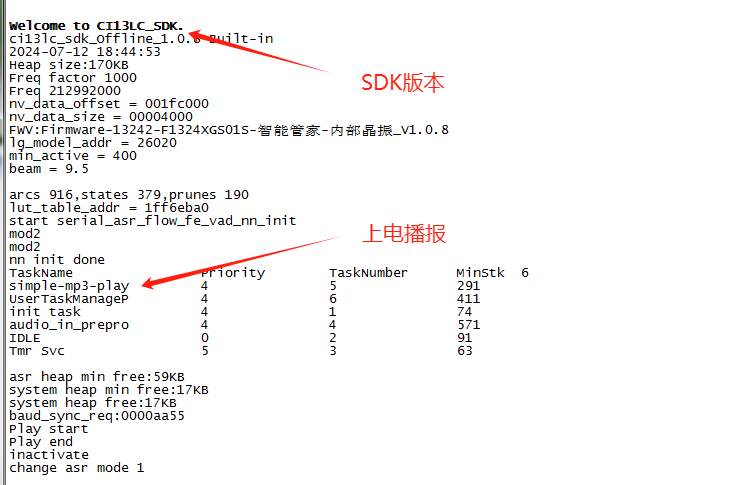
When applying this module, install it on the baseboard or host motherboard and connect external speakers and microphones. The module will start after applying 5V power. After normal power-on, the speaker will play a startup prompt tone, and the UART0 port will output print information. Users can connect the UART0 port to a computer using tools such as a USB-to-TTL Tool and view the print information in the computer’s serial debugging window. The appearance of print information as shown in Figure 8 indicates that the module has started normally.
Note: The UART0 interface of the module is a 3.3V high-speed serial port, which also supports direct communication with 5V level signals without requiring level conversion circuitry.
The module requires an external 5V power supply for normal operation. Pins 8 and 17 of the module (optimal for power input) are both 5V power input interfaces. The power amplifier chip also uses a 5V power supply. The rated power supply current for 5V should be guaranteed to be above 500mA, with stable power supply and ripple within 300mV.
Module Default Command Words
Mass-produced modules with custom firmware will be pre-loaded with the firmware specified by the customer before leaving the factory.
Modules with our company’s standard firmware will be pre-loaded with our standard firmware and its inherent command words for user testing. The standard firmware command words are shown in the following figure:

Module Default Serial Communication Protocol
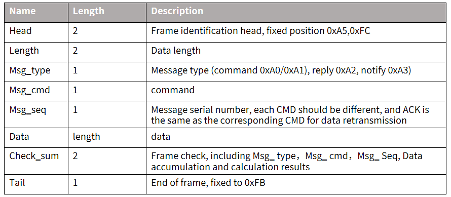
Modules with standard firmware support serial communication for communication with MCUs or connected systems. This serial protocol is extensible and has the following features:
- Complete transmission packet, including: header, tail, length, checksum, message type, and message sequence number.
- Supports variable-length commands for easy expansion.
- Message types (command, notification, response).
- Command messages are configurable with ACK responses. Notification messages do not have ACK.
- The message format will be the same as that used for bootloader upgrades, distinguished from the bootloader protocol by the header.
- Default baud rate is 9600.
- Note: The module only reserves the UART0 interface, which defaults to a print output interface. If UART0 is to be used as the serial protocol interface mentioned above, the code must be modified. Refer to the serial protocol section of the ☞CI13LC Series Chip SDK documentation for implementation details.
- Supported commands: Query protocol version, query system version, set volume (volume levels are defined in user_config.h), play local notification sounds, reset command, etc. The specific protocol format is shown in the following figure:
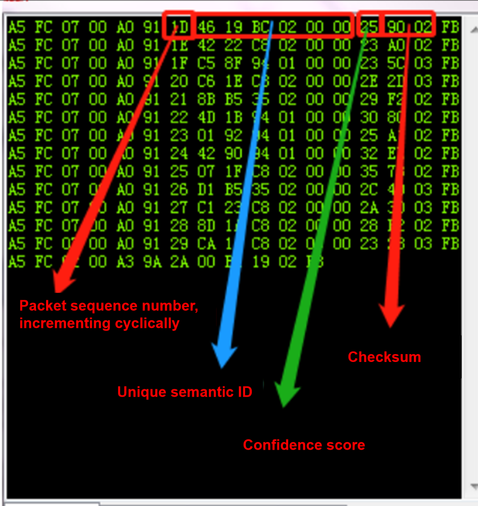
Example 1:
A5 FC 07 00 A0 91 18 01 55 E0 01 00 00 1B 9B 02 FB is parsed as follows:
A5 FC: Head
07 00: 7 bytes of valid data
A0: This is command word information
91: Command number 0x91 (this data content is command word data)
18: Packet sequence number, the 0x08th data transmission from this serial port, this value increments continuously
01 55 E0 01 00 00: semantic ID, UNIQUE
1B: Command word threshold
9B 02: Checksum
FB: End data
Note: If only the command word and threshold are of interest in the application, only the 7 bytes of valid data in the blue part need to be focused on.
Example 2:
A5 FC 02 00 A3 9A 17 00 B1 05 02 FB is parsed as follows:
A5 FC: Head
02 00: 2 bytes of valid data
A3: This is notification data
9A: Command number 0x9A (this data content indicates voice module content change)
17: The 0x07th data transmission from this serial port, this value increments continuously
00 B1: Valid data (this data indicates entering wake-up state)
05 02: Checksum
FB: End data
Note: This is notification data, and users can choose to use this information as needed.
For more data parsing content, please refer to the serial protocol section in ☞CI13LC Series Chip SDK. The following figure shows a reference screenshot of protocol data:
Software Development
The default firmware included with the module is primarily for initial user experience. For software development, users need to register and log in to the Chipintelli AI Speech Development Platform (https://aiplatform.Chipintelli.com) for rapid voice firmware development. Additionally, the “Development Resources” section of the Chipintelli AI Speech Development Platform allows for downloading the SDK and related hardware documentation.
For first-time users of the Chipintelli AI Speech Development Platform, it is recommended to start with the Beginner’s Guide to understand the specific development process. You can also refer to the documentation center’s Video Tutorials for more solutions and SDK development introduction.
The software development process mainly includes the following steps:
- SDK development package download
- Model generation(language model + acoustic model)
- Voice synthesis
- Association of command word information table with audio files
- Firmware packaging
For detailed development process, please click ☞CI13LC Series Chip SDK to learn more.
Firmware Flashing
Pre-Flashing Preparation
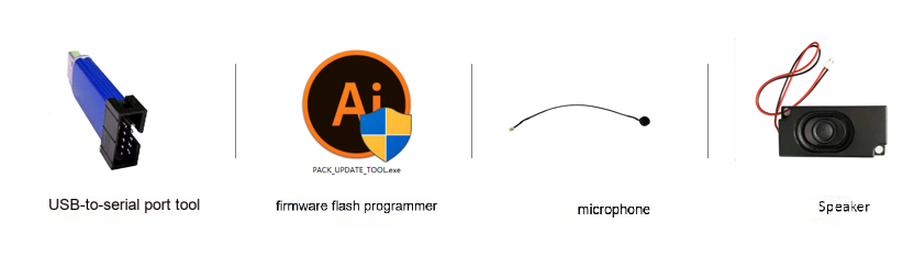
Before flashing the module, prepare the following tools and items:
- Module to be flashed
- USB-to-serial converter
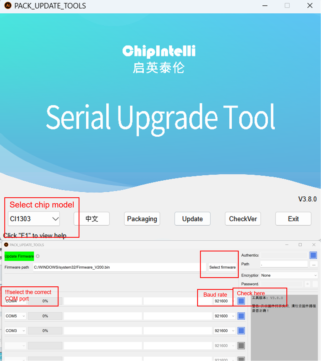
- Firmware flashing tool (pack_update_tool.exe)
- Firmware file (*.bin format)
- Microphone and speaker matching the interface of the baseboard/MCU
- Several DuPont wires
Hardware Connection and Flashing
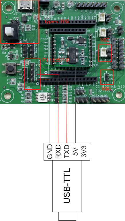
Taking the USB-to-serial converter shown in the figure above as an example, before flashing, connect the power, ground, and serial communication pins of the USB-to-serial converter to the corresponding pins of the module. (Note: The RXD and TXD of the USB-to-serial converter correspond to UART0_TX and UART0_RX of the module, respectively.) The connection method is shown in the figure below.
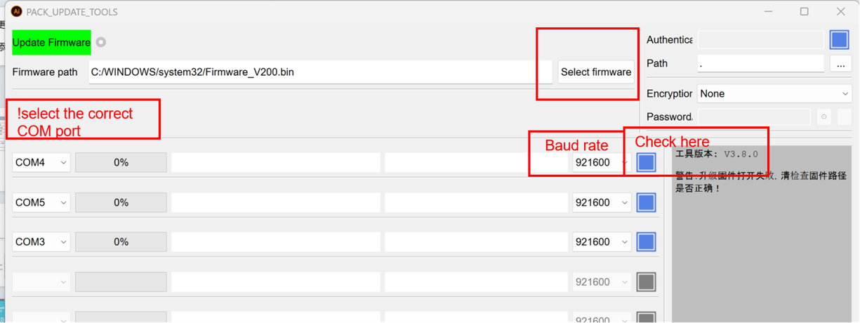
Open the firmware flashing tool (this tool can be found in the CI13LC_SDK\tools directory of the SDK development package), select the corresponding chip model, click the Firmware Update button, select the prepared firmware file, and confirm the COM port number assigned by the computer to the USB-to-serial converter. After powering on the module, it will enter the Firmware Update mode and start downloading the firmware. If the computer cannot recognize the USB-to-serial converter, please install the corresponding driver first. (The module is upgraded on the baseboard.)
Functional Testing After flashing
After the firmware flashing is completed, functional testing of the module is required to confirm whether the firmware flashing was successful. Before functional testing, connect the microphone and speaker to the module to be tested, power it on to confirm whether the power-on prompt sound is played, and test whether it can be woken up and recognized normally using wake words and command words. If all functions work normally, the module flashing is successful; otherwise, the flashing has failed, and the cause of the failure needs to be identified.
Possible Issues and Solutions During Use
This section lists some issues that may be encountered during module use and their corresponding solutions.
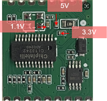
- Module cannot flash firmware If this issue occurs, perform the following checks in order: 1. Check if the serial port pins are connected correctly, if TX and RX are reversed, if the USB-to-serial converter driver on the computer is functioning properly, and if the correct COM port is selected in the PC flashing tool. 2. Check if the module power is connected properly or if there is any short circuit. 3. If the above checks are correct but the module still cannot be flashed, use a multimeter to measure the module’s power supply voltages (5V, 3.3V, 1.1V) for accuracy. The voltage measurement points are shown in the figure below. If any voltage abnormalities are found, please replace the module or perform further circuit repairs. If necessary, contact our technical support for assistance.
- No broadcast after successful firmware flashing and power-on If this issue occurs, check the following points: 1. Confirm that the module is powered normally and the speaker is connected correctly. 2. Verify that the flashed firmware is compatible with the module. 3. Use an oscilloscope to measure the voice output test point of the main chip (as shown in the figure below). If no output waveform is detected when there should be voice output, check if the firmware is correct. If there is an output waveform, check if there are any soldering issues with the power amplifier on the module or if the power amplifier itself is faulty. If the issue persists after these checks, please contact our technical support for assistance.
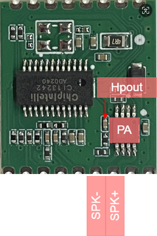
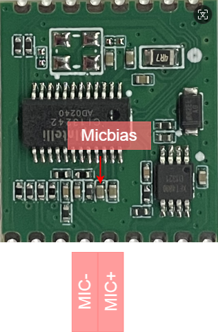
- Module has audio output after flashing but does not recognize command words If this issue occurs, perform the following checks in order: 1. Check if the microphone is connected correctly. 2. Verify that the microphone’s polarity matches the markings on the module. 3. Use a multimeter to measure if the MICBIAS pin of the main chip has a voltage of approximately 2.8V. Use an oscilloscope to check if there is an input voice waveform on the microphone input pin (set the oscilloscope to 100mV per division). If the signal is normal, consider whether the firmware is correct. If the signal is abnormal, check if there is any physical damage to the module hardware. The measurement points are shown in the figure below. If the issue persists after these checks, please contact our technical support for assistance.
Other Application Notes
-
The CI13241 & CI13242 chips have a high ESD level, and the module is designed to be easily expandable for users. Therefore, the module only includes ESD protection on the microphone. For products with higher ESD requirements, additional ESD protection devices can be added. It is recommended to wear anti-static wristbands, anti-static gloves, or fingerless gloves during inspection and production processes. Please reserve space for ESD protection devices at the corresponding bottom board connector positions to ensure product quality and reliability.
-
The microphone, speaker, power supply, and serial port interfaces of the module must be connected correctly.
-
If you need to use a USB-to-serial converter to debug the module, you need to add serial port print commands in the corresponding positions of the SDK program, compile it to generate firmware and flash it, and then you can debug and verify it.
-
All IO ports of the module support both 3.3V and 5V communication levels.
-
When designing the module bottom board or MCU motherboard, the module 5V power input port needs to be configured with a capacitor with a capacitance of no less than 100uF, and the microphone signal line should be as short as possible and pay attention to shielding. The SPK signal line should be as short and thick as possible, and there should be no other lines crossing over in the area where the signal line is laid and the PCB backside.
-
The curvature of the control board should not exceed 0.5%, to prevent the module from being welded poorly.
Production Guide, Storage and Ordering Information
Production Storage Guide
-
CI-F24XGS01S modules must be soldered using SMT machines (except for pin-type soldering), and must be soldered within 24 hours after opening.
-
CI-F24XGS01S modules storage conditions are as follows:
- Modules packaged in vacuum moisture-proof bags can be stored in a storage environment with a temperature range of -40℃-+100℃ and a humidity range of 0%-85% RH.
- The vacuum moisture-proof bag is equipped with a humidity indicator card as shown in the figure:

- If the humidity indicator card shows the following color changes, the modules need to be baked according to the corresponding baking parameters:
- When the vacuum bag is opened, if the humidity indicator card shows that the blue rings of the 30%, 40%, and 50% values are all blue, the modules need to be baked for 2 hours.
- If the humidity indicator card shows that the 30% ring turns pink, the modules need to be baked for 4 hours.
- If the humidity indicator card shows that the 30% and 40% rings turn pink, the modules need to be baked for 6 hours.
- If the humidity indicator card shows that the 30%, 40%, and 50% rings turn pink, the modules need to be baked for 12 hours.
- Baking parameters are as follows:
- Baking temperature: 125±5℃
- Alarm temperature setting: 130℃
- Baking times: 1 time
- Natural cooling, module temperature <36℃ after cooling, then SMT can be performed
- If the module is not soldered within 12 hours after baking, it needs to be baked again.
- The entire soldering operation process needs to be protected against ESD, and production operations need to wear anti-static gloves.
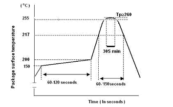
Recommended Reflow Profile
Ordering Information
| Product Model | Packaging Method | Number of Modules per Tray | Number of Modules per Package | Number of Modules per Box |
|---|---|---|---|---|
| CI-F241GS01S CI-F242GS01S |
Tray + Anti-static bag + Carton | 140pcs | 15 trays 2100pcs | 3 bags 6300pcs |
Purchase and Technical Support
If you want to purchase our products samples, please click ☞Samples Purchase , you can also click ☞Samples and Sample and Bulk Purchase to get more information.
If you want to get technical support, please login ☞Chipintelli AI Platform .