Pin Diagram and Functional Description
Pin Diagram
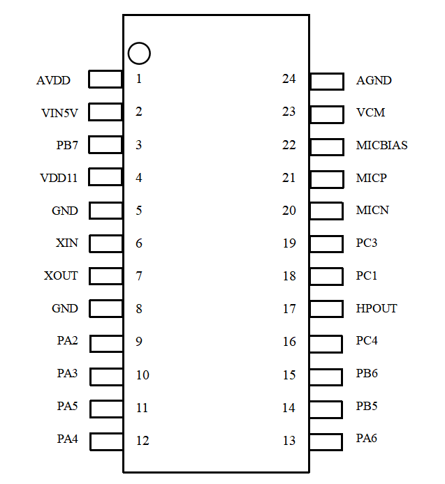
Pin Description
| Pin No. | Pin Name | Type | 5V Tolerant | Default State | Pin Function |
|---|---|---|---|---|---|
| 1 | AVDD | P | - | - | ● Internal LDO-3.3V output ● 3.3V power supply input for analog circuits Note1 |
| 2 | VIN5V | P | - | - | ● Power supply input, 3.6V~5.5V operating range Note1 |
| 3 | PB7 | IO | - | IN,T+U | ● GPIO PB7 |
| 4 | VDD11 | P | - | - | 1.1V LDO output pin, also serves as core power supply input, requires external 4.7uF capacitor |
| 5 | GND | P | - | - | Ground pin |
| 6 | XIN | I | - | - | ● XIN (default state at power-on) ● GPIO PA0 ● PWM2 |
| 7 | XOUT | O | - | - | ● XOUT (default state at power-on) ● GPIO PA1 |
| 8 | GND | P | - | - | Ground pin |
| 9 | PA2 | IO | √ | IN,T+D | ● GPIO PA2 (default state at power-on) ● IIS_SDI ● I2C_SDA ● UART1_TX ● PWM0 ● PWMP |
| 10 | PA3 | IO | √ | IN,T+D | ● GPIO PA3 (default state at power-on) ● IIS_LRCLK ● I2C_SCL ● UART1_RX1 ● PWM1 ● PWMN |
| 11 | PA5 | IO | √ | IN,T+D | ● GPIO PA5 (default state at power-on) ● IIS_SCLK ● - ● UART2_TX ● PWM3 ● PWMN0 |
| 12 | PA4 | IO | √ | IN,T+U | ● GPIO PA4 (default state at power-on)/PG_EN (programming mode enable, high level at power-on enables programming mode) ● IIS_SDO ● - ● - ● PWM2 ● PWMP |
| 13 | PA6 | IO | √ | IN,T+D | ● GPIO PA6 (default state at power-on) ● IIS_MCLK ● - ● UART2_RX ● PWM0 |
| 14 | PB5 | IO | √ | IN,T+U | ● GPIO PB5 (default state at power-on) ● UART0_TX ● I2C_SDA ● PWM1 ● PWMP |
| 15 | PB6 | IO | √ | IN,T+U | ● GPIO PB6 (default state at power-on) ● UART0_RX ● I2C_SCL ● PWM2 ● PWMN |
| 16 | PC4 | IO | - | IN,T+U | ● Reserved (default state at power-on) G ● PC4 ● SCL ● PWM0 |
| 17 | HPOUT | O | - | - | DAC output |
| 18 | PC1 | I0 | - | IN,T+D | ● Reserved (default state at power-on) ● GPIO PC1 ● TX2 ● PWM3 |
| 19 | PC3 | I0 | - | IN,T+D | ● Reserved (default state at power-on) ● GPIO PC3 ● SDA ● PWM1 |
| 20 | MICNL | I | - | - | Left Microphone N input |
| 21 | MICPL | I | - | - | Left Microphone P input |
| 22 | MICBIAS | O | - | - | Microphone bias output |
| 23 | VCM | O | - | - | VCM Output |
| 24 | AGND | P | - | - | Analog ground |
Note1: This pin requires an external 4.7uF capacitor
Note2: When this pin is high at power-on, the system will enter programming mode
Symbol Definitions
I Input
O Output
IO Bidirectional
P Power or Ground
T+D Tri-state with pull-down
T+U Tri-state with pull-up
OUT Default to output mode at power-on
IN Default to input mode at power-on
All IOs support configurable drive strength and pull-up/down resistors.
Multiplexing Functions
| Pin Name | Function1 | Function2 | Function3 | Function4 | Function5 | Function6 | Specific Function |
|---|---|---|---|---|---|---|---|
| PA0 | PA0 | PWM2 | - | - | - | - | XIN |
| PA1 | XOUT | ||||||
| PA2 | PA2 | - | I2C_SDA | UART1_TX | PWM0 | PWMP | - |
| PA3 | PA3 | - | I2C_SCL | UART1_RX | PWM1 | PWMN | - |
| PA4 | PA4 | - | - | - | PWM2 | - | PG_EN Note3 |
| PA5 | PA5 | SCLK | TX2 | PWM3 | PWMN | ||
| PA6 | PA6 | MCLK | RX2 | PWM0 | |||
| PB5 | PB5 | UART0_TX | I2C_SDA | PWM1 | PWMP | - | - |
| PB6 | PB6 | UART0_RX | I2C_SCL | PWM2 | PWMN | - | - |
| PC4 | - | PC4 | SCL | PWM0 | |||
| PC1 | - | PC1 | TX2 | PWM3 | |||
| PC3 | - | PC3 | SDA | PWM1 |
Note3: The PA4 (PG_EN) pin has an internal pull-up by default. When the system detects this pin is high at power-on and there is a Firmware Update signal on the UART0 interface, it will automatically enter upgrade mode, allowing programming of the internal Flash via the upgrade tool. If no Firmware Update signal is detected on the UART0 interface or if the PA4 pin voltage is low, the system will enter normal operation mode.