Pin Diagram and Functional Description
Pin Diagram
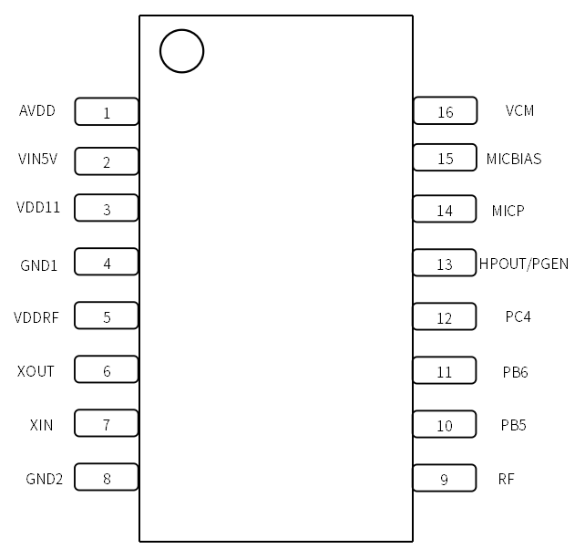
Figure P-1 Pin Assignment and Definition
Pin Description
Table P-1 Pin Description
| Pin No. | Pin Name | Type | 5V Tolerant | Default State | Pin Function |
|---|---|---|---|---|---|
| 1 | AVDD | P | - | - | ● Internal LDO-3.3V Output ● 3.3V Power Supply for Analog Circuits Note1 |
| 2 | VIN5V | P | - | - | ● Power Supply Input (3.6V - 5.5V) Note1 |
| 3 | VDD11 | P | - | - | ● LDO-1.1V Output ● 1.1V Core Power Supply Note1 |
| 4 | GND1 | P | - | - | Ground |
| 5 | VDDRF | P | - | - | ● RF Power Input |
| 6 | XOUT | IO | - | - | ● Crystal Oscillator Output |
| 7 | XIN | IO | - | - | ● Crystal Oscillator Input |
| 8 | GND2 | P | - | - | Ground |
| 9 | RF | IO | - | - | ● RF Antenna |
| 10 | PB5 | IO | √ | IN,T+U | ● GPIO PB5 (Default) ● UART0_TX ● I2C_SDA ● PWM1 ● PWMP |
| 11 | PB6 | IO | √ | IN,T+U | ● GPIO PB6 (Default) ● UART0_RX ● I2C_SCL ● PWM2 ● PWMN |
| 12 | PC4 | IO | - | IN,T+U | ● Reserved (Default: GND) ● PC4 ● SCL ● PWM0 |
| 13 | HPOUT | O | - | - | DAC Output Note2 |
| 14 | MICP | I | - | - | Microphone Positive Input |
| 15 | MICBIAS | O | - | - | Microphone Bias Output |
| 16 | VCM | O | - | - | VCM Output |
Note1: Requires external 4.7μF capacitor
Note2: System enters programming mode when this pin is high during power-up
Symbol Definitions
I - Input
O - Output
IO - Bidirectional
P - Power or Ground
T+D - Tri-state with Pull-down
T+U - Tri-state with Pull-up
OUT - Default to output mode at power-up
IN - Default to input mode at power-up
All IOs support configurable drive strength and pull-up/down resistors.
Multiplexed Functions
Table P-2 IO Multiplexing Functions
| Pin Number | Function1 | Function2 | Function3 | Function4 | Function5 | Function6 | Specific Function |
|---|---|---|---|---|---|---|---|
| PB5 | PB5 | UART0_TX | I2C_SDA | PWM1 | PWMP | - | - |
| PB6 | PB6 | UART0_RX | I2C_SCL | PWM2 | PWMN | - | - |
| PC4 | - | PC4 | SCL | PWM0 | - | - | - |