Hardware Design
The CI13082V chip requires minimal external components to develop end-product solutions supporting various voice applications. The chip supports single-ended microphone input. The application design can be tailored based on functional requirements, power consumption, cost, and other factors to select the most suitable circuit design solution.
This document uses the typical application solution of CI13082V as an example to introduce the key points and considerations for application design:
Reference Circuit Diagram
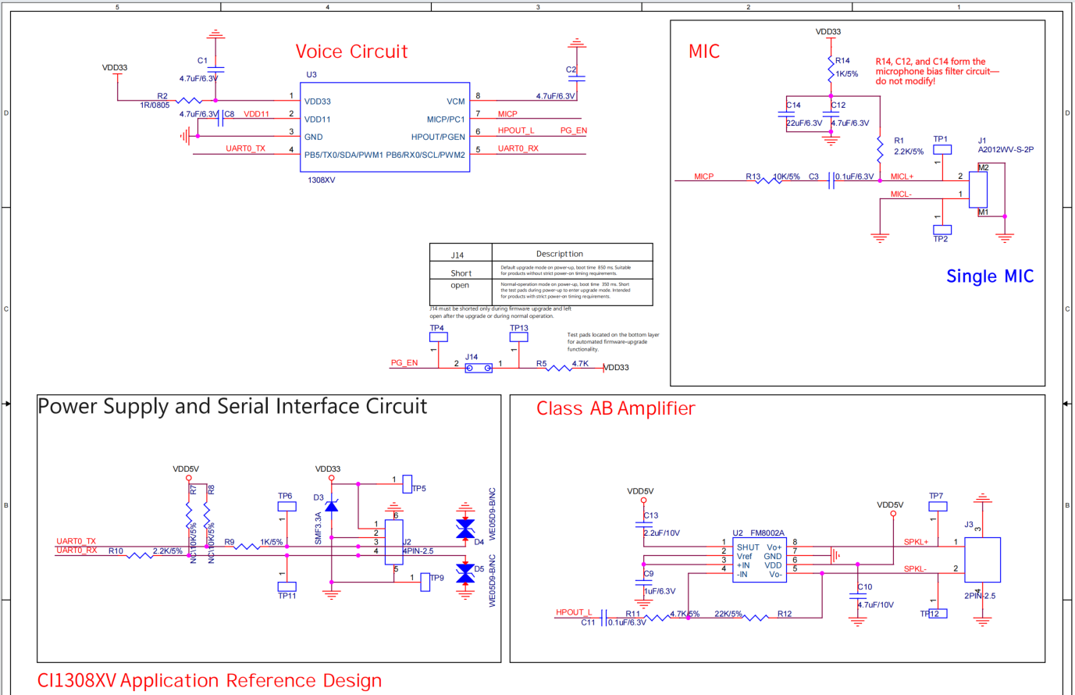
The reference design circuit diagram shows a typical application solution for CI13082V with single-ended microphone input and power amplifier output. This design is not limited to any specific end product. The application design should be based on the principle of adapting to the host terminal product. According to the functional and performance requirements of the end product, please visit ChipIntelli’s documentation center and AI platform to download reference schematics and PCB layouts. Documentation Center: https://document.chipintelli.com/.
To reserve board-level upgrade functionality in the application design, the UART0 pins can be brought out via connectors or test points, facilitating firmware programming or upgrades through UART0 after PCB assembly.
The HPOUT/PGEN pin of CI13082V has an internal pull-down resistor. During power-up, the system detects whether this pin is pulled high to 3.3V by an external pull-up resistor. If it is high and an upgrade signal is detected on the UART0 pins, the system enters upgrade mode. If no external pull-up resistor is connected, the chip can skip the upgrade mode detection and directly enter normal boot mode for faster startup. For applications requiring fast startup, the HPOUT/PGEN pin can be brought out with a jumper and connected to VDD33 through a 4.7KΩ resistor. In this configuration, the system powers up in normal functional mode with a startup time of approximately 350ms. For in-system upgrades, the PGEN pin can be pulled high to 3.3V by shorting the jumper or test points, enabling upgrades via the UART0 interface. If fast startup is not required, PGEN can be directly pulled high through a 4.7KΩ resistor. For specific implementation details, please refer to the reference application diagram or consult our FAE. The two working modes of PGEN are shown in the following table:
| PG_EN Working Mode Diagram | J14 Configuration | PG_EN Level | Boot Time |
|---|---|---|---|
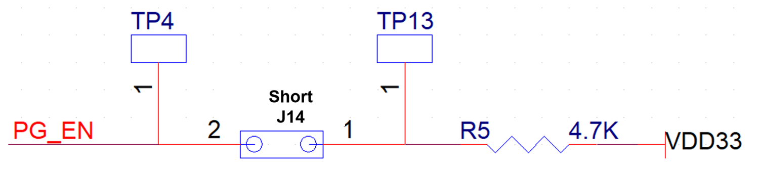 |
Shorted | High, Upgrade Mode | 850ms |
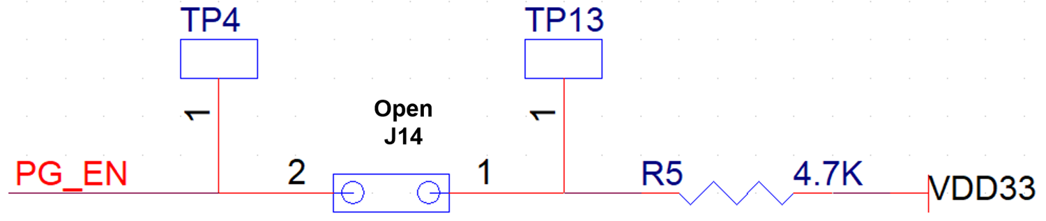 |
Open | Low, Normal Mode | 350ms |
The CI13082V chip does not have a MICBIAS pin. The microphone is powered by an external 3.3V supply. It is recommended to use the power supply design shown in Figure 6-1, where the filter circuit consisting of R14, C12, and C14 must not be modified.
CI13082V only supports single-ended microphone input. It is recommended to use the microphone design shown in Figure H-1, with a trace length of less than 20cm.
This typical application uses a Class AB power amplifier configuration, with the 8002 series amplifier recommended. If voice playback functionality is not required, this circuit can be removed to reduce solution cost. For power amplifier MUTE functionality, please refer to Figure H-1.
The UART interface of CI13082V supports 5V level communication. For applications requiring 5V level communication, it is recommended to use the UART design shown in Figure H-1, where 5V pull-up resistors are added to the RX and TX pins of UART0 without requiring level conversion circuitry.
ChipIntelli provides various reference schematic solutions to meet most common application scenarios. In actual application development, customers should carefully select the most suitable reference schematic based on specific product functional requirements, system characteristics, and application scenarios for reference and design optimization. As ChipIntelli cannot be familiar with all product systems and application knowledge, we recommend that customers or solution partners conduct comprehensive testing and verification of product functionality (including the compatibility of voice chips/modules with the product system) in combination with the product system and application scenarios before mass production. If there are any unclear or uncertain issues during the design modification process, please contact ChipIntelli’s FAE engineers for thorough communication. The reference solution list is as follows:
| Solution Name | Functionality | Application Scenario | Documentation Link |
|---|---|---|---|
| Typical Solution | Simplest circuit with single-mic single-ended input, without AEC | Widely applicable to various conventional end products, supports voice prompts | ☞Typical Application Solution Reference Design |
PCB Layout Design
Power Circuit
Power Traces
Pay attention to overvoltage and surge protection for power input. Include TVS devices and 1Ω resistors in the 3.3V input, with traces passing through the TVS first, then the resistor before reaching the chip. The width of power traces should be determined by the actual circuit current. The trace width for 3.3V power should be no less than 15 mils, and for 1.1V power, no less than 15 mils. Use copper pour for power traces when possible, keeping them as short and wide as possible. The narrowest part of power traces should not be less than 8 mils, and avoid forming closed loops in power traces.
Power Decoupling Capacitors
Place power decoupling capacitors as close as possible to their corresponding pins.
ESD Protection Requirements
For two-layer board designs, try to route traces on the TOP layer to maintain the integrity of the BOTTOM ground plane. If ESD protection devices are included in the design, place them as close as possible to the connector pins to enhance protection effectiveness.
Additional Application Notes
-
CI13082V is manufactured with lead-free, environmentally friendly materials. When performing SMT soldering, please set the reflow temperature and time parameters according to lead-free standards. A typical SMT soldering temperature profile is shown below:
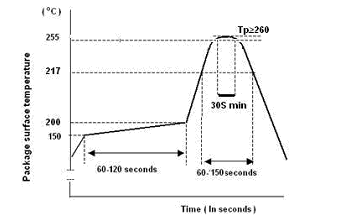 Figure H-2 Chip SMT Soldering Temperature Profile
 -
Implement ESD protection measures during handling, transportation, and production of CI13082V. Use anti-static packaging materials.
-
The chip has a moisture sensitivity level (MSL) of 3. Store the device under MSL3 conditions before use. If the package has been opened and stored longer than the MSL3 requirements, bake the device before SMT soldering.