Interface Description
General Purpose Input/Output (GPIO)
Introduction
GPIO (General Purpose I/O) is a versatile input/output port that enables devices to interact with peripheral hardware through level signals. It can function as an input to receive external signals or as an output to control peripheral hardware.
Features
CI13082V supports multiple programmable input/output pins (individually configurable via software), with each GPIO port having corresponding control and configuration registers. This allows individual enabling/disabling of each GPIO pin for precise control and status monitoring of peripheral hardware. The CI13082V chip supports 2 GPIO groups (GPIO1, GPIO2), where GPIO1 corresponds to the chip’s PB port and GPIO2 corresponds to the PC port. For the pin assignment of each GPIO group, please refer to section 2.2 Pin Description.
CI13082V provides various interfaces including: - I/O status query interface - Interrupt masking interface - Interrupt mask query interface - Interrupt clear interface - Interrupt status query interface - Interrupt trigger configuration interface (configurable as: low-level trigger, high-level trigger, rising edge trigger, falling edge trigger, or both-edge trigger)
These features are designed to meet different application scenarios and requirements.
Universal Asynchronous Receiver/Transmitter (UART)
Introduction
UART (Universal Asynchronous Receiver/Transmitter) is a general-purpose asynchronous serial communication interface that enables data transmission and reception between two devices, supporting full-duplex communication. Since there is no shared clock signal between the transmitter and receiver, both communicating devices must be configured with the same baud rate and data frame format to ensure reliable communication.
The CI13082V supports 1 UART controller: UART0.
Features
- Supports standard UART protocol with configurable data frame format consisting of: start bit, data bits (configurable length), optional parity bit, and stop bits (configurable width). Also supports configurable baud rate.
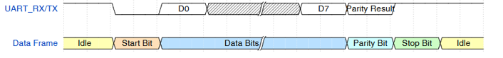
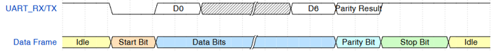
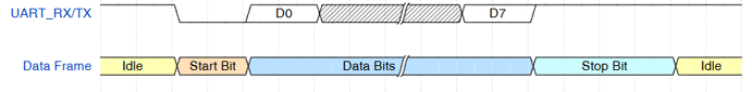
- The signal line remains in high level when the bus is idle.
- Start Bit: Marks the beginning of a data frame. Each frame starts with a low-level signal of one bit width from the transmitter, notifying the receiver that data transmission has begun.
- Data Bits: The data length can be configured from 5 to 8 bits through the UART_LCR register. 8 bits is commonly used. Data is transmitted LSB (Least Significant Bit) first, with the LSB sent first and the MSB (Most Significant Bit) last.
- Parity Bit: The UART_LCR register is used to enable/disable parity checking and to configure it as odd or even parity. When parity checking is enabled, errors in data transmission can be detected after the data bits are transmitted.
- Stop Bit(s): Marks the end of a data frame, with the line returning to high level. The stop bit length can be configured as 1, 1.5, or 2 bits through the UART_LCR register.
Timing Diagrams
Timing diagram for UART data transmission of one data frame (8 data bits, parity bit, 1 stop bit):
Timing diagram for UART data transmission of one data frame (start bit, 7 data bits, parity bit, 1.5 stop bits):
Timing diagram for UART data transmission of one data frame (start bit, 8 data bits, no parity bit, 2 stop bits):
Higher UART baud rates enable faster data transmission but may increase interference and bit error rates. When setting the baud rate, it’s important to ensure that both communicating devices’ UART hardware supports the selected rate. Excessively high baud rates may lead to unstable data transmission.
The maximum supported baud rate is 3Mbps, configurable through the UART_I_BRD and UART_F_BRD registers.
Pulse Width Modulation (PWM)
Introduction
PWM (Pulse Width Modulation) is a technique that modulates the duty cycle (the ratio of high-level time to the total period) of digital pulses to simulate analog signal levels. It is widely used in motor control, power management, LED dimming, and other fields.
The CI13082V features 4 dedicated PWM channels. The frequency of each PWM output signal is configured through the TIMER_SC register, and the duty cycle is set via the TIMER_SPWMC register. Note that 100% duty cycle (constant high) is not supported. If a 100% duty cycle is required, it can be achieved by configuring a GPIO pin instead.
Features
- Clock prescaler support with division ratios of 1, 2, 4, and 16, configurable through the TIMER_CFG register.
- Supports two 32-bit down-counters.
- Variable duty cycle PWM pulse width waveform output.
- Configurable output level polarity after stopping through the TIMER_RESTART_MD register.
General-Purpose Timer (TIMER)
Introduction
The TIMER (General-Purpose Timer) is a 32-bit down-counter based on a configurable prescaler and multiple counting modes. It triggers a timer event when the count value reaches 0, commonly used for generating periodic interrupts or as an event counter at specified time intervals. The CI13082V features 2 identical dedicated timers: TIMER0 and TIMER1, which support timer cascading.
Features
- Three counting modes configurable through the TIMER_CFG register:
- One-shot mode: The timer counts for only one counting cycle.
- Auto-reload mode: The counter is automatically reloaded with the initial value at the end of each counting cycle.
-
Free-running mode: The counter rolls over from 0xFFFFFFFF to 0x00000000 at the end of each counting cycle.
-
Clock prescaler with division ratios of 1, 2, 4, and 16, configurable through the TIMER_CFG register.
- 32-bit down-counter with the ability to read the real-time counter value through the TIMER_CC register.
- Cascade mode configuration supported through the TIMER_CFG0 register.
- Interrupt generation upon counter completion.
Inter-Integrated Circuit (I²C) Bus
Introduction
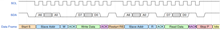
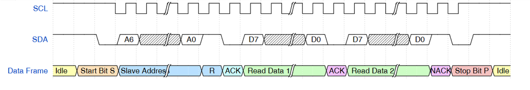
I²C (Inter-Integrated Circuit) is a bidirectional two-wire synchronous serial bus consisting of SDA (Serial Data Line) and SCL (Serial Clock Line), with both SDA and SCL pins configured as open-drain outputs. The I²C bus is typically used for communication between one or more master devices and one or more slave devices. Each device connected to the bus has a unique address, and only one master device is allowed to initiate access to a slave device at any given time.
The CI13082V supports 1 I²C interface. Its data frame format typically consists of five parts: start condition, address signal, acknowledge signal, data signal, and stop condition. It supports two transmission modes: standard mode at 100 kbit/s and fast mode at 400 kbit/s.
Feature Description
- SDA: Serial Data Line, bidirectional I/O line
- SCL: Serial Clock Line, provided by the master device
- Configurable as either master or slave mode through registers
- Master: When operating as master, it initiates data transfer on the bus and generates the clock signal
- Slave: When operating as slave, it responds when addressed with its unique address
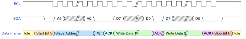
- Start Condition: SDA transitions from high to low while SCL is high, indicating the start of transmission
- Address Signal: Supports 7-bit addressing mode, including 7 address bits and 1 read/write bit
- Acknowledge Signal: ACK indicates successful reception, NACK indicates reception failure or end of transmission
- Data Signal: Transmitted in bytes, with the Most Significant Bit (MSB) sent first and the Least Significant Bit (LSB) last
- Stop Condition: SDA transitions from low to high while SCL is high, indicating the end of transmission
- Configurable bus transmission rates: Standard (100 kbit/s) and Fast (400 kbit/s)
Timing Diagrams
Communication is initiated by the master device generating a Start condition: pulling SDA low while SCL is high, followed by 8 clock pulses on SCL to transmit one byte containing 7 address bits and 1 read/write bit. If a slave device’s address matches the transmitted 7-bit address, it generates an acknowledge signal. Both master and slave devices determine whether to send or receive data based on the read/write bit, and the logical level of the acknowledge bit indicates whether to terminate the data transfer. During data transmission, SDA only changes when SCL is low. Upon completion of communication, the master device sends a STOP condition to end the communication: pulling SDA high while SCL is high.
Independent Watchdog (IWDG)
Introduction
The IWDG (Independent Watchdog) is a hardware timing circuit primarily used to detect system failures caused by operational anomalies and facilitate recovery from such faults.
Features
The CI13082V features 1 IWDG module. The IWDG is based on a 32-bit down-counter that decrements from a loaded value. When the counter reaches zero, it generates a timeout interrupt and reloads the initial value. If the timeout interrupt is not cleared by the time the counter reaches zero again, the IWDG will generate a reset request.
The reset domain range can be configured through the SYS_RESET_CFG register.
Multimedia Audio CODEC
Introduction
The CI13082V integrates a high-performance, low-power audio CODEC that supports one ADC channel and one DAC channel. The analog signal from the MIC input first passes through a MIC gain stage and is then amplified by a PGA (Programmable Gain Amplifier). This PGA can be controlled by the CODEC’s built-in ALC (Automatic Level Control). After the PGA stage, additional digital gain can be applied for further amplification.
Features
- DAC: Supports up to 24-bit resolution with SNR up to 90dB
- ADC: Supports up to 24-bit resolution with SNR up to 90dB
- Input Support: Single-ended and differential MIC inputs, line-in inputs
- ALC: Built-in Automatic Level Control for gain adjustment
- Sampling Rates: 8kHz, 12kHz, 16kHz, 24kHz, 32kHz, 44.1kHz, 48kHz
Enhanced Pulse Width Modulation (EPWM)
Introduction
EPWM (Enhanced Pulse Width Modulation) is a more sophisticated pulse width modulation technology compared to standard PWM, offering enhanced functionality and configuration options. It supports special features such as inversion, chopping, and specific phase control for both low and high levels. Widely used in industrial and consumer electronics power control applications, including motor control and switch-mode power supplies.
Each EPWM module consists of two PWM outputs: PWMN and PWMP. This pair of PWM outputs can be used independently as standard PWM, complementary PWM, or customized PWM outputs.
Features
- 16-bit frequency-controllable counter
- Configurable counter start/stop via external signals or software through the TBCTL register
- Supports multiple PWM output modes for the output pair:
- Center-aligned PWM
- Edge-aligned PWM
- Asymmetric edge-aligned PWM
- Configurable initial phase through the TBPHS register
- 16-bit dead-band timing with configurable rising/falling edge delays via DBRED/DBFED registers
- Configurable PWM output states (high, low, or high-impedance) during fault conditions through the TZSEL register
Configuration Parameters
Key configuration parameters for EPWM include TBPRD, ZERO, CMPA, and CMPB. TBPRD defines the PWM period length, while CMPA and CMPB set the duty cycle. These parameters control both the frequency and duty cycle of the PWM output.
- TBPRD: Period value (>0), up to 16 bits. Configures actions (set high, set low, or no change) when counter reaches TBPRD via AQCTLA or AQCTLB registers.
- ZERO: Zero-crossing value (=0). Configures actions when counter reaches zero via AQCTLA or AQCTLB registers.
- CMPA: Compare value A, up to 16 bits. Configures actions when counter matches CMPA via AQCTLA or AQCTLB registers.
- CMPB: Compare value B, up to 16 bits. Configures actions when counter matches CMPB via AQCTLA or AQCTLB registers.
Counting Modes
EPWM supports three counting modes, each suitable for different application scenarios:
- Up-counting mode: Counter increments from 0 to TBPRD in each period. One PWM period is completed in one TBPRD cycle. Configured via TBCTR register.
- Down-counting mode: Counter decrements from TBPRD to 0 in each period. One PWM period is completed in one TBPRD cycle. Configured via TBCTR register.
- Up-down counting mode: Counter increments from 0 to TBPRD in odd-numbered periods and decrements from TBPRD to 0 in even-numbered periods. One PWM period is completed in two TBPRD cycles. Configured via TBCTR register.
Usage Method
EPWM can generate various waveforms through configuration, such as 50% duty cycle PWM or low-duty-cycle PWM. To achieve the desired waveform, follow these steps: 1. Configure the values of TBPRD, CMPA, and CMPB 2. Select the appropriate counting mode 3. Configure the actions to be taken when the counter reaches TBPRD, ZERO, CMPA, and CMPB
Note: The configuration allows for CMPA = CMPB, CMPA > CMPB, or CMPA < CMPB to achieve different waveform outputs.