Pin Diagram and Functional Description
Pinout Diagram
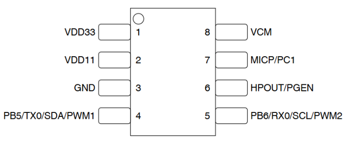
Pin Description
| Pin Number | Pin Name | Type | 5V Tolerant | Power-on Default State | Pin Function |
|---|---|---|---|---|---|
| 1 | VDD33 | P | - | - | ● Power supply voltage input, range 3.0V~3.6V Note1 |
| 2 | VDD11 | P | - | - | ● 1.1V LDO output pin, also serves as core power supply input, requires external 4.7uF capacitor |
| 3 | GND | P | - | - | Ground pin |
| 4 | PB5 | IO | √ | IN,T+U | ● GPIO PB5 (default at power-on) ● UART0_TX ● IIC_SDA ● PWM1 ● PWMP |
| 5 | PB6 | IO | √ | IN,T+U | ● GPIO PB6 (default at power-on) ● UART0_RX ● IIC_SCL ● PWM2 ● PWMN |
| 6 | HPOUT | IO | - | IN,T+D | ● DAC output ● PC0 ● - ● - ● PWM0 ● PGEN Note2 |
| 7 | MICP | I | - | - | ● Microphone P input |
| 8 | VCM | P | - | - | ● VCM voltage, requires external 4.7uF capacitor |
Note1: This pin requires an external 4.7uF capacitor
Note2: System enters programming mode when this pin is high during power-on
Symbol Definitions
I Input
O Output
IO Bidirectional
P Power or Ground
T+D Tri-state with pull-down
T+U Tri-state with pull-up
OUT Default to output mode at power-on
IN Default to input mode at power-on
All IOs support configurable drive strength and pull-up/down resistors.
Multiplexing Functions
| Pin Name | Function1 | Function2 | Function3 | Function4 | Function5 | Function6 | Specific Function |
|---|---|---|---|---|---|---|---|
| PB5 | PB5 | UART0_TX | IIC_SDA | PWM1 | PWMP | - | - |
| PB6 | PB6 | UART0_RX | IIC_SCL | PWM2 | PWMN | - | - |
| PC1 | - | PC1 | TX2 | PWM3 | - | - | - |
| PC0 Note3 |
PC0 | - | - | PWM0 | - | - | PGEN |
Note3: HPOUT is multiplexed with PC0 (PGEN) pin, internally pulled down by default. The function can be configured by software after power-on. When the system detects a high level on this pin during power-on and there is a firmware update signal on the UART0 interface, it will automatically enter the update mode, allowing programming of the internal Flash via the update tool. If the system does not detect a firmware update signal on the UART0 interface or detects a low level on the PC0 pin, it will enter normal operation mode.