Hardware Design
The CI2316X chip requires minimal external components to develop end-product solutions supporting various voice applications. The chip supports single-ended microphone input. The application design can be tailored based on functional requirements, power consumption, cost, and other factors.
This section uses the CI23162 typical application as an example to introduce key design points and considerations:
Reference Circuit Diagram
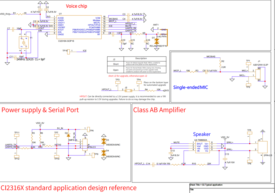
The above diagram shows the reference design circuit for the CI2316X series chips (including CI23162), featuring single-ended microphone input and power amplifier output. This design is not limited to any specific end product. Application designs should be based on the principle of adapting to the host terminal product. For reference schematics and PCB layouts, please visit Chipintelli’s Documentation Center and AI Platform: https://document.Chipintelli.com/.
To reserve board-level upgrade functionality, the UART0 pins can be exposed via headers or test points, allowing firmware programming or upgrades through UART0 after PCB assembly.
The HPOUT/PGEN pin of CI23162 has an internal pull-down resistor. During power-up, the system checks if this pin is pulled high to 3.3V by an external pull-up resistor. If high and an upgrade signal is detected on the UART0 pins, the system enters upgrade mode. If no external pull-up is connected, the system skips the upgrade mode detection and boots directly into normal operation for faster startup.
For applications requiring fast boot time, the HPOUT/PGEN pin can be connected to a 3.3V supply through a 4.7KΩ resistor with a jumper. In this configuration, the system starts in normal mode with a boot time of approximately 350ms. For Firmware Updates, short the jumper to pull PGEN high to 3.3V, enabling upgrade mode via UART0. If fast boot is not required, PGEN can be permanently pulled high through a 4.7KΩ resistor. Refer to the reference design or consult our FAE for implementation details. The two PGEN operating modes are as follows:
| J4 Connection | PG_EN Level | Boot Time |
|---|---|---|
| Open | Low | 350ms |
| Shorted | High | 850ms |
CI23162 supports single-ended microphone input, with the configuration shown in Figure H-1 recommended.
The reference design uses a Class AB power amplifier (8002 series recommended). Remove this circuit if voice playback is not required to reduce cost.
For applications without ultra-low power requirements, use the internal PMU for power supply to reduce cost. For ultra-low power applications, use an external DCDC converter to supply 1.1V to CI23162.
All UART ports on CI23162 support 5V level communication. The UART0 interface in the diagram shows 3.3V level communication. For 5V level communication, add 5V pull-up resistors to the RX and TX pins; no level shifter is required.
PCB Layout Design
Power Circuit
Power Traces
Implement overvoltage and surge protection at the 5V input with a TVS device and 1Ω resistor. Route the power trace through the TVS first, then the resistor before reaching the chip. Trace width should be determined by current requirements, with minimum widths of 15 mil for 3.3V and 1.1V power rails. Use copper pours where possible, keeping power traces short and wide. The minimum trace width should not be less than 8 mil. Avoid creating power loops.
Power Decoupling Capacitors
Place decoupling capacitors as close as possible to their corresponding pins.
ESD Protection Requirements
For two-layer board designs, route signals on the top layer and maintain a solid ground plane on the bottom layer. Place ESD protection devices as close as possible to the connector pins for optimal protection.
Additional Application Notes
-
CI2316X is manufactured using lead-free materials. Follow lead-free reflow profiles for SMT assembly. The recommended reflow temperature profile is shown below:
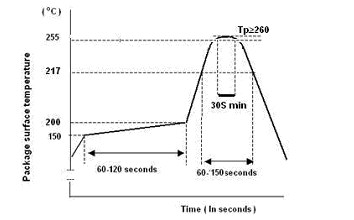 Figure H-2 Chip SMT Reflow Temperature Profile
 -
Handle CI2316X with appropriate ESD precautions during all stages of handling, assembly, and production. Use ESD-safe packaging materials.
-
The chip has a Moisture Sensitivity Level (MSL) of 3. Store under MSL3 conditions before use. If the package has been exposed beyond MSL3 limits, bake the components before SMT assembly.