Pin Diagram and Functional Description
Pin Diagram
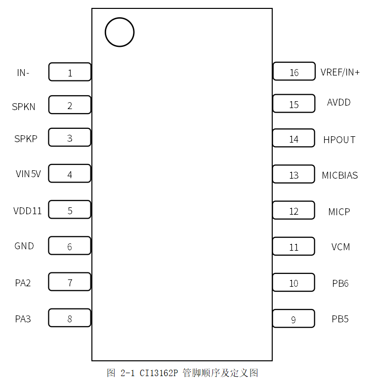
Figure P-1 Pin Sequence and Definition Diagram
Pin Description
Table P-1 Pin Description
| Pin No. | Pin Name | Type | 5V Tolerant | Default State | Pin Function |
|---|---|---|---|---|---|
| 1 | IN- | IO | - | - | ● Inverting input of power amplifier |
| 2 | SPKN | IO | - | - | ● Negative output of power amplifier |
| 3 | SPKP | IO | - | - | ● Positive output of power amplifier |
| 4 | VIN5V | P | - | - | ● Power supply input, 3.6V~5.5V Note1 |
| 5 | VDD11 | P | - | - | ● LDO-1.1V output ● Core 1.1V power supply input Note1 |
| 6 | GND | P | - | - | Ground |
| 7 | PA2 | IO | √ | IN,T+D | ● GPIO PA2 (default state) ● IIS_SDI ● IIC_SDA ● UART1_TX ● PWM0 ● PWMP |
| 8 | PA3 | IO | √ | IN,T+D | ● GPIO PA3 (default state) ● IIS_LRCLK ● IIC_SCL ● UART1_RX1 ● PWM1 ● PWMN |
| 9 | PB5 | IO | √ | IN,T+U | ● GPIO PB5 (default state) ● UART0_TX ● IIC_SDA ● PWM1 ● PWMP |
| 10 | PB6 | IO | √ | IN,T+U | ● GPIO PB6 (default state) ● UART0_RX ● IIC_SCL ● PWM2 ● PWMN |
| 11 | VCM | O | - | - | ● VCM Output ● PGEN Note2 |
| 12 | MICP | I | - | - | Microphone P input |
| 13 | MICBIAS | O | - | - | Microphone bias output |
| 14 | HPOUT | O | - | - | DAC output |
| 15 | AVDD | P | - | - | ● Internal LDO-3.3V output ● 3.3V power supply for internal analog circuits Note1 |
| 16 | VREF/IN+ | IO | - | - | ● Reference voltage for power amplifier |
Note1: A 4.7μF capacitor should be connected to this pin
Note2: When this pin is high at power-on, the system will enter programming mode
Symbol Definitions
I Input
O Output
IO Bidirectional
P Power or Ground
T+D Tri-state with pull-down
T+U Tri-state with pull-up
OUT Default to output mode at power-on
IN Default to input mode at power-on
All IOs support configurable drive capability and pull-up/down resistors.
Multiplexing Functions
Table P-2 IO Multiplexing Functions
| Pin Number | Function1 | Function2 | Function3 | Function4 | Function5 | Function6 | Specific Function |
|---|---|---|---|---|---|---|---|
| PA2 | PA2 | - | IIC_SDA | UART1_TX | PWM0 | PWMP | - |
| PA3 | PA3 | - | IIC_SCL | UART1_RX | PWM1 | PWMN | - |
| PB5 | PB5 | UART0_TX | IIC_SDA | PWM1 | PWMP | - | - |
| PB6 | PB6 | UART0_RX | IIC_SCL | PWM2 | PWMN | - | - |